Driving circuit for power semiconductor element

A technology of power semiconductors and drive circuits, which is applied in the manufacture of semiconductor devices, electrical components, semiconductor/solid-state devices, etc. It can solve the problems of short-circuit detection lag and failure to protect IGBT1, and achieve the effects of improving reliability and preventing malfunctions

Inactive Publication Date: 2004-02-18
NEXGEN CONTROL SYST LLC
View PDF0 Cites 27 Cited by
  • Summary
  • Abstract
  • Description
  • Claims
  • Application Information

AI Technical Summary

Problems solved by technology

For this reason, the short-circuit detection by the collector voltage detection circuit 6 is significantly delayed, and there is a problem that the IGBT1 may not be protected.

Method used


Image

  • Driving circuit for power semiconductor element
  • Driving circuit for power semiconductor element
  • Driving circuit for power semiconductor element

Examples


Embodiment Construction

[0056] One embodiment of the present invention will be described below.

[0057] Embodiment 1

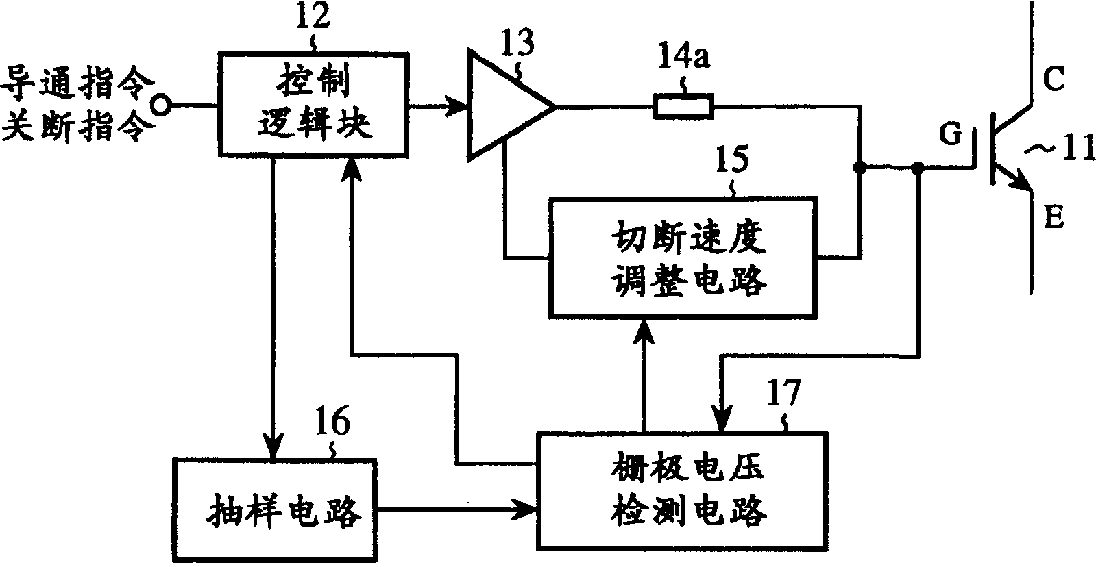
[0058] figure 1 It is a configuration diagram showing the drive circuit of the power semiconductor element according to Embodiment 1 of the present invention, and in the figure, 11 is an IGBT (insulated gate bipolar transistor) as the power semiconductor element. Here, the power semiconductor element is not limited to IGBT, and may be a voltage-driven semiconductor element such as MOSFET, for example.

[0059] 12 is a gate command to turn on the IGBT11 is output to the buffer 13 if an on command is input from the outside, and a gate command to turn off the IGBT11 is output to the buffer 13 if an off command is input from the outside. The control logic block, 13 is a buffer for driving the IGBT11 according to the gate command output from the control logic block 12, 14a is a turn-on gate resistance, and 15 is the IGBT11 that is turned off according to the detection of an abnormalit...


PUM


Abstract

When it is applied to the IGBT1 with high withstand voltage, it is necessary to connect the diodes 5 with high withstand voltage in series in multiple stages, and there is a problem of high cost or reduced reliability. In addition, the collector voltage detection circuit 6 performs Short-circuit detection lags significantly, and there is a problem that sometimes the IGBT1 cannot be protected. The solution is that the sampling circuit 16 detects the gate voltage Vge during the detection processing period of the allowable gate voltage Vge, and if the gate voltage Vge exceeds the reference value, It is determined that an abnormality has occurred in the IGBT11.

Description

technical field [0001] The present invention relates to a driving circuit of a power semiconductor element for detecting an abnormality occurring in the power semiconductor element. Background technique [0002] Figure 24 It is a structural diagram showing a drive circuit of a conventional power semiconductor element. In the figure, 1 is an IGBT (Insulated Gate Bipolar Transistor) as a power semiconductor element, and 2 is a switch to switch IGBT1 when a conduction command is input from the outside. The gate command to the closed state is output to the buffer 3, and if the shut-off command is input from the outside, the gate command to transfer the IGBT1 to the open state is output to the control logic block of the buffer 3, and 3 is based on the slave control logic The gate command output by block 2 drives the buffer of IGBT1, 4a is the turn-on gate resistance, 4b is the turn-off gate resistance, 5 is the cathode connected to the collector of IGBT1, and the anode is connec...

Claims


Application Information

Patent Timeline
Patent Type & Authority Applications(China)
IPC IPC(8): H01L27/04H01L21/822H02M1/00H02M1/08H03K17/0812H03K17/16
CPCH03K17/08128H03K17/168
Inventor 大井健史中山靖田中毅
Owner NEXGEN CONTROL SYST LLC
Why Eureka
Try Eureka