Duty degree correction circuit and delayed phase-lock loop having same

A technology for correcting circuits and duty cycles, applied in the field of delay-locked loops, which can solve problems such as occupation, power consumption, and multi-chip area

Inactive Publication Date: 2004-05-26
CONVERSANT IP N B 868
View PDF0 Cites 12 Cited by
  • Summary
  • Abstract
  • Description
  • Claims
  • Application Information

AI Technical Summary

Problems solved by technology

[0016] However, conventional DCC circuits have some disadvantages
As shown in Figure 2, the DCC circuit is an analog circuit, so it consumes a lot of power
In addition, the DCC circuit must be placed before and after the delay line of the DLL, thus occupying too much die area

Method used


Image

  • Duty degree correction circuit and delayed phase-lock loop having same
  • Duty degree correction circuit and delayed phase-lock loop having same
  • Duty degree correction circuit and delayed phase-lock loop having same

Examples


Embodiment Construction

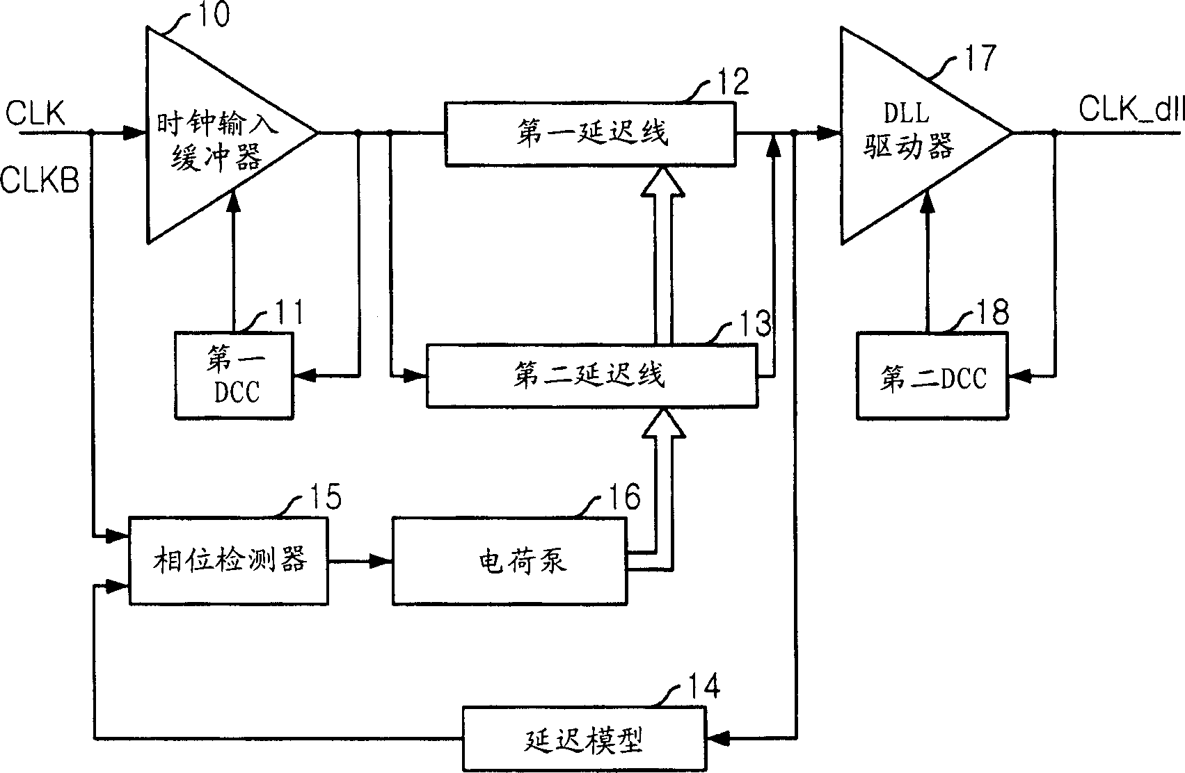
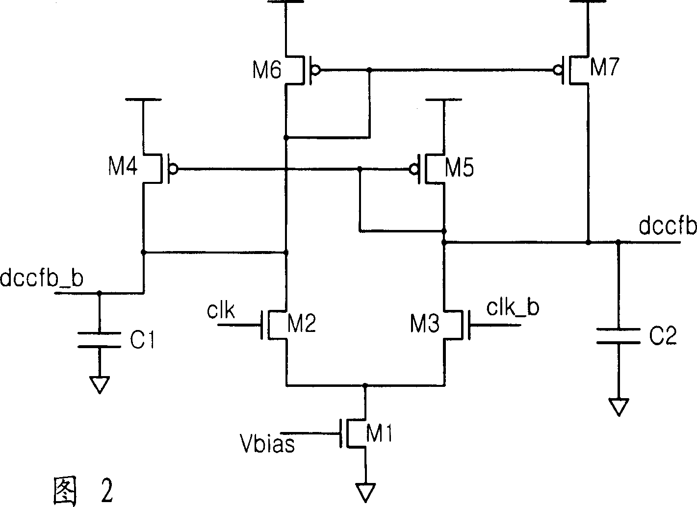
[0025] Hereinafter, a duty cycle correction circuit (DCC) and a delay locked loop (DLL) including the duty cycle correction circuit of the present invention will be described in detail with reference to the accompanying drawings.

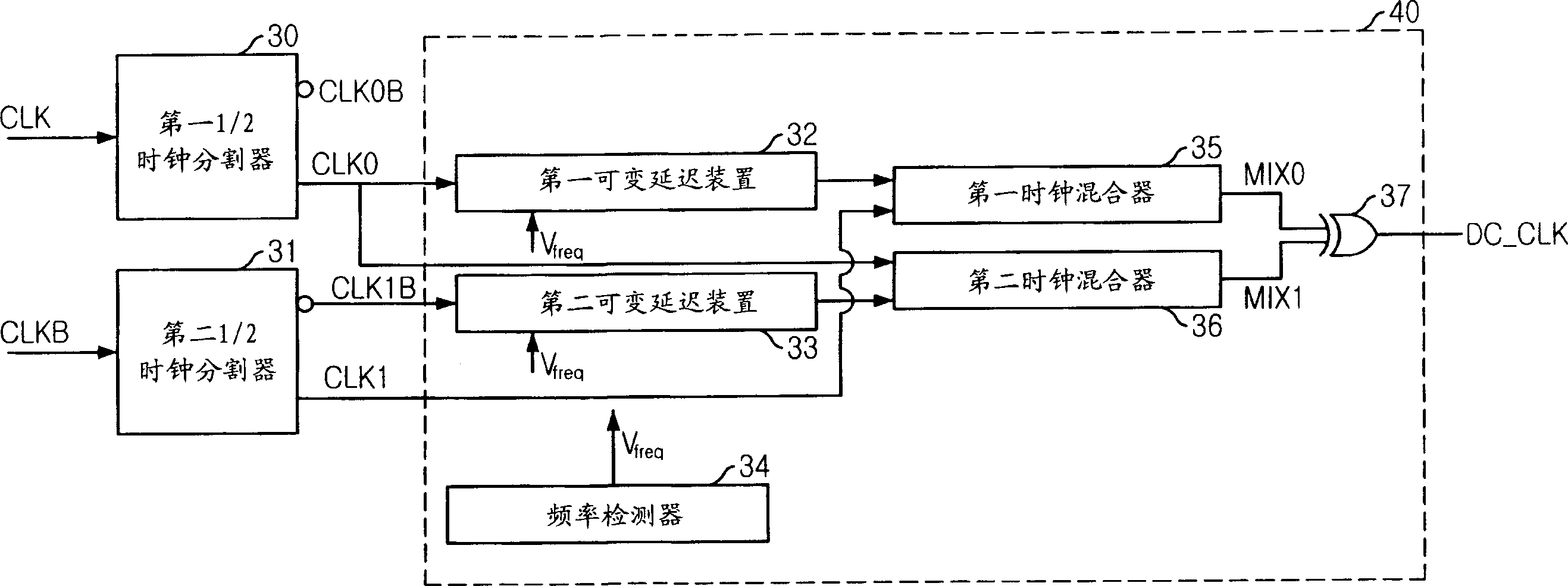
[0026] image 3 is a block diagram of a DCC circuit according to a preferred embodiment of the present invention.

[0027] refer to image 3 , the DCC circuit includes: a first 1 / 2 clock divider 30 for generating normal split clocks (CLK0 and CLK0B) by dividing a normal input clock (CLK) by 2; a second 1 / 2 clock divider device 31 for generating clocks (CLK1 and CLK1B) by dividing a sub-normal input clock (CLKB) by 2; and a DCC core circuit 40 for dividing The duty cycle of the output of the device 31 is used to generate a duty cycle corrected clock (DC_CLK) having a corrected duty cycle.

[0028] The core circuit 40 includes: a frequency detector 34, which is used to generate a voltage signal (Vfreq) that varies proportionally to the frequency of...


PUM


Abstract

The present invention provides a duty cycle correction circuit (DCC) and a delay locked loop (DLL) including the same. The inventive duty cycle correction circuit includes: a first clock dividing unit and a second clock dividing unit for dividing an ordinary input clock and a sub ordinary input clock; a first clock mixing unit; a second clock mixing unit; and a logic combination unit for generating a duty cycle correction clock. In addition, the inventive delay locked loop (DLL) includes: a first and second clock dividing unit; a frequency detecting unit; a first variable delaying unit; a second variable delaying unit; a first clock mixing unit; a second clock mixing unit; and a logic combination unit.

Description

technical field [0001] The present invention relates to a semiconductor circuit, more specifically to a duty cycle correction circuit (DCC, duty cycle correction) and a delay locked loop (DLL, delay locked loop) having the duty cycle correction circuit . Background technique [0002] In general, the timing of operations can be adjusted using a clock as a reference. This clock can also be used to ensure higher speed operation without any errors. When an external clock input from the outside is used as an internal clock in an internal circuit, a time delay will occur in the internal circuit. The time delay between the external clock and the internal clock can be compensated by using a DLL so that the internal clock and the external clock have the same phase. [0003] Also, DLLs are less susceptible to noise than traditional phase-locked loops (PLLs). Therefore, DLLs can generally be used for double data rate synchronous DRAM (DDR SDRAM) as well as synchronous semiconductor...

Claims


Application Information

Patent Timeline
Patent Type & Authority Applications(China)
IPC IPC(8): H03L7/08H03K5/156H03L7/081H03L7/089
CPCH03K5/1565H03L7/0812H03L7/0805H03L7/0891H03L7/0816H03L7/08
Inventor 洪祥熏金世埈鞠廷勋
Owner CONVERSANT IP N B 868
Why Eureka
Try Eureka