Method for eliminating height difference between metal lugs on wafer and crystal grain

A metal bump, wafer technology, applied in electrical components, semiconductor/solid-state device manufacturing, circuits, etc., can solve problems such as reduced efficiency

Inactive Publication Date: 2004-08-11
CHIPBOND TECH
View PDF0 Cites 4 Cited by
  • Summary
  • Abstract
  • Description
  • Claims
  • Application Information

AI Technical Summary

Problems solved by technology

like figure 1 Height differences in ΔX

Method used


Image

  • Method for eliminating height difference between metal lugs on wafer and crystal grain
  • Method for eliminating height difference between metal lugs on wafer and crystal grain
  • Method for eliminating height difference between metal lugs on wafer and crystal grain

Examples


Embodiment Construction

[0023] The present invention provides several methods to substantially eliminate the height difference between a plurality of metal bumps on the wafer and the crystal grain, so as to achieve the effect of flattening the metal bumps.

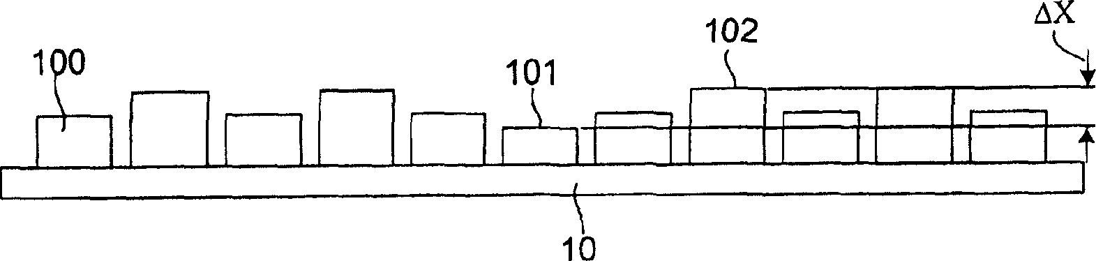
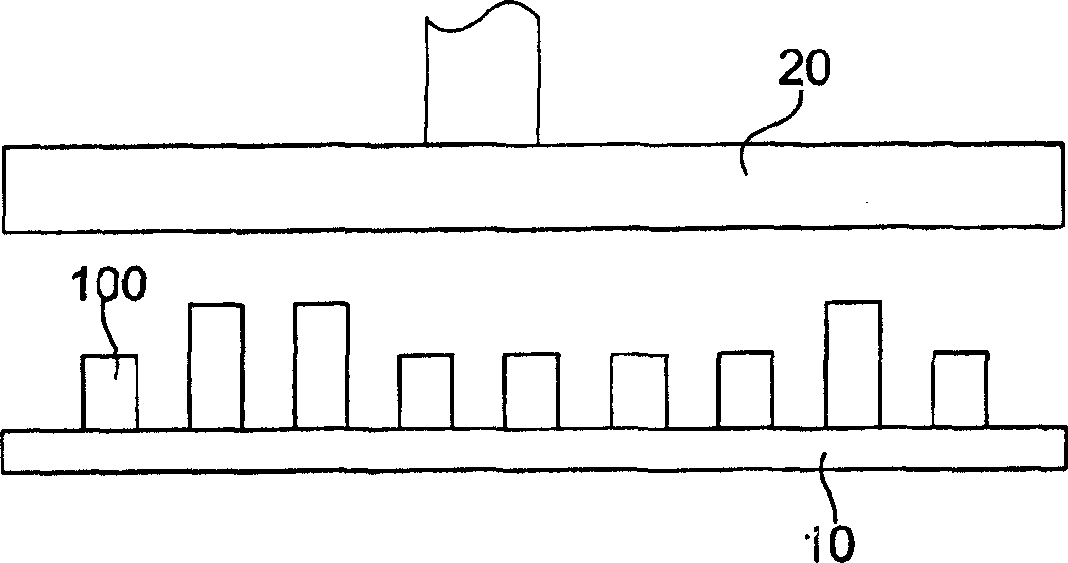
[0024] When the wafer or die has such figure 1 The height difference of the metal bump 100 can be determined by such as Figure 2A to Figure 2C The method is used to achieve the planarization effect of the metal bump. In the first embodiment of the present invention, the pressing device (not shown) has a flat pressing plate 20, such as Figure 2A shown. The planar platen 20 is aligned with the wafer or die 10 , so that the planar platen 20 is aligned with the area on the wafer or die 10 where height differences among the plurality of metal bumps 100 need to be eliminated.

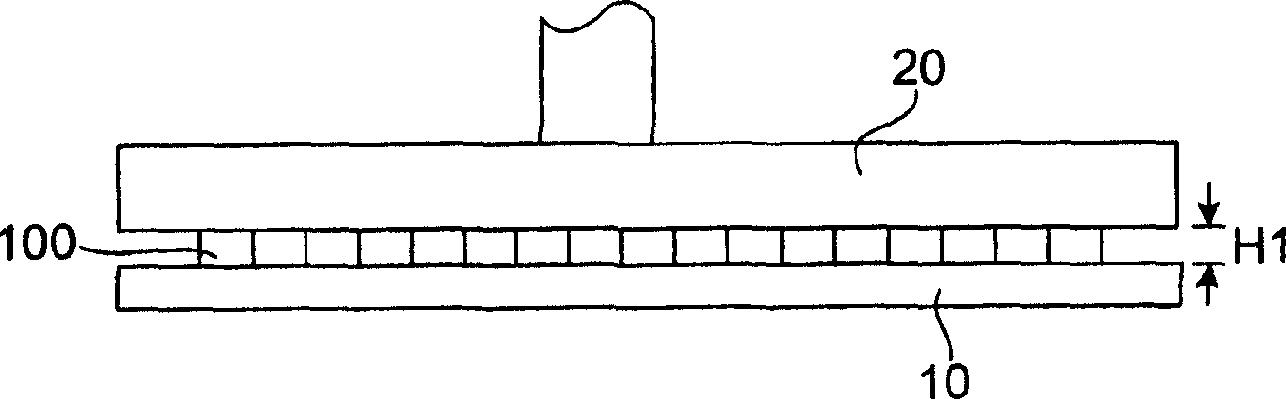
[0025] Figure 2B Among them, the flat platen 20 presses the wafer or die 10 to a predetermined height H1, and the predetermined height H1 refers to the distance between t...


PUM


Abstract

Using pressurized method or combining with grinding method can eliminate height difference among all metal lugs throughout piece of wafer, and on crystal grains at one process, so as to make all metal lugs possess same height substantially.

Description

technical field [0001] The present invention relates to a method for eliminating the height difference between metal bumps on wafers and dies. Background technique [0002] With current bump manufacturing technology, it is always difficult to control the planarization and height uniformity of all metal bumps on a wafer or die. The main reason is that the current density during electroplating and the concentration of the electroplating solution are not easy to control. Also because of this, the height of metal bumps cannot be effectively controlled no matter within a single wafer (within wafer), or between two wafers (wafer-wafer) or between crystal grains. [0003] Please refer to figure 1 , there are a plurality of metal bumps 100 on the wafer or die 10 . Due to the inhomogeneity of the aforementioned metal bump manufacturing process, among the plurality of metal bumps 100 there will be the metal bump 101 with the lowest height and the metal bump 102 with the highest hei...

Claims


Application Information

Patent Timeline
IPC IPC(8): H01L21/304H01L21/463
Inventor 吴非艰
Owner CHIPBOND TECH
Why Eureka
Try Eureka