800G silicon optical module

A silicon photonics and silicon photonics chip technology, applied in the field of optical communication, can solve the problems of long gold wire bonding length, high-speed performance cannot be effectively guaranteed, and PCB circuit board strength is not satisfactory.

Pending Publication Date: 2021-09-10
HENGTONG ROCKLEY TECHNOLOGY CO LTD
View PDF1 Cites 2 Cited by
  • Summary
  • Abstract
  • Description
  • Claims
  • Application Information

AI Technical Summary

Problems solved by technology

[0004] Based on the silicon photonics technology under the background of the current optical module industry, the thickness of the silicon photonics chip is generally thick, and there is a certain height difference between the electrical chip and the silicon photonics chip, resulting in a long bonding length of the gold wire, and the high-speed performance cannot be effectively guaranteed
If the height difference between the electrical chip and the silicon photonic chip is eliminated by digging grooves on the PCB circuit board, it will inevitably cause the problem of insufficient strength of the PCB circuit board. Module, which improves the strength of the PCB circuit board by thickening the PCB circuit board. However, the non-standardized PCB circuit board used in this way also increases the production cost of the optical module. At the same time, due to the design problem of the slotting of the PCB circuit board, among them The strength of the PCB circuit board is still not satisfactory

Method used


Image

  • 800G silicon optical module
  • 800G silicon optical module
  • 800G silicon optical module

Examples


Embodiment Construction

[0022] The technical solution of the present invention will be clearly and completely described below in conjunction with the accompanying drawings. The relevant components in the invention are not drawn according to the number, shape and size of the components in actual implementation. The type, quantity and proportion of each component in actual implementation can be changed arbitrarily, and the layout of the components may also be changed for complex.

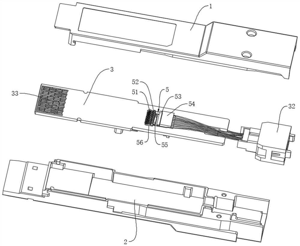
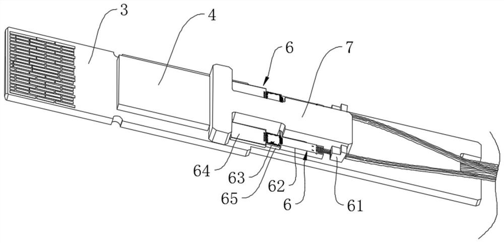
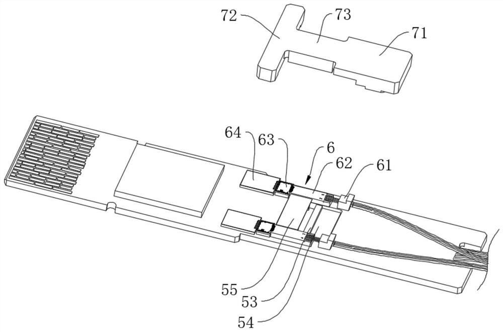
[0023] An 800G silicon optical module of the present invention includes an upper case 1, a lower case 2 that can be spliced ​​into one, and a PCB circuit board 3 arranged between the upper case 1 and the lower case 2, and the PCB circuit board 3 A control chip 4, a transmitting end component 5, and a receiving end component 6 are provided, and the middle slot of the PCB circuit board 3 constitutes a transmitting end layout area 31, and the transmitting end component 5 is placed in the transmitting end layout area 31, and the...


PUM


Abstract

The present invention provides a 800G silicon optical module which is reasonable in structural layout, the strength of a PCB (Printed Circuit Board) can still be ensured under the condition that the PCB with a standard design is adopted, meanwhile, the production cost is low, a slot is formed in the middle of the PCB to form a transmitting end arrangement area, a transmitting end component is arranged in the transmitting end arrangement area, and the transmitting end component is arranged in the transmitting end arrangement area. The metal heat sink is upwards attached to the transmitting end assembly from the lower surface of the PCB, the lower surface of the PCB is provided with a control chip and a receiving end assembly avoiding the metal heat sink, and the receiving end assembly comprises an optical fiber array, a silicon optical chip, an electric chip and a ceramic substrate which are sequentially arranged. The silicon optical chip, the electric chip and the ceramic substrate are bonded through gold threads, and the electric chip is installed on the PCB through a metal cushion block so that the electric chip, the silicon optical chip and the ceramic substrate can be arranged at the same height.

Description

technical field [0001] The invention relates to the technical field of optical communication, in particular to an 800G silicon optical module. Background technique [0002] With the continuous and rapid development of my country's optical communication industry and the renewal and upgrading of communication technology, optical modules, as the basis for building modern high-speed information networks, play a vital role in the optical communication industry, and their continuous development is an inevitable trend. [0003] The current development of optical modules is mainly manifested in high speed and high density. On the basis of the continuous increase in the speed of optical chips, the number of them is also increasing, so as to ensure the transmission rate of optical modules. The current 800G optical module supporting circuits are complex, and there are many types and quantities of electronic components. Compared with traditional photonic technology, optical modules usin...

Claims


Application Information

Patent Timeline
Patent Type & Authority Applications(China)
IPC IPC(8): G02B6/42
CPCG02B6/428G02B6/4274G02B6/4245
Inventor 丁晓亮甘飞尤炎炎梁巍王志勇陈奔朱宇李量
Owner HENGTONG ROCKLEY TECHNOLOGY CO LTD
Why Eureka
Try Eureka