Wafer level chip scale package of image sensor and manufacturing method thereof

a scale package and image sensor technology, applied in the direction of semiconductor devices, semiconductor/solid-state device details, radiation control devices, etc., can solve the problems of low connection reliability, large structural difficulty in stacking the wafer level chip scale package or applying it to manufacture the sensor package, and complex structure and process. , to achieve the effect of improving production capacity, reducing the number of foreign particles, and improving the quality of the packag

Inactive Publication Date: 2011-11-08
SAMSUNG ELECTRO MECHANICS CO LTD
View PDF22 Cites 5 Cited by
  • Summary
  • Abstract
  • Description
  • Claims
  • Application Information

AI Technical Summary

Benefits of technology

[0022]An advantage of the present invention is that it provides a wafer level chip scale package of an image sensor and a manufacturing method thereof. In the wafer level chip scale package of the image sensor, since expansion pads instead of solder balls are provided, a complicated process of forming solder balls can be omitted, thereby improving production capability. Since a glass is attached in a wafer level, defects caused by foreign particles can be minimized. Furthermore, miniaturization and slimness of the package can be realized.
[0023]Additional aspects and advantages of the present general inventive concept will be set forth in part in the description which follows and, in part, will be obvious from the description, or may be learned by practice of the general inventive concept.
[0024]According to an aspect of the invention, a wafer level chip scale package of an image sensor includes: a wafer including an image sensor and a pad on the top surface thereof and inclined surfaces on both ends thereof; expansion pads formed on the inclined surfaces of the wafer, including the pad, such that the expansion pads are electrically connected to the pad, the expansion pads having a bottom surface on a straight line with respect to that of the wafer; a support formed on the expansion pads to support both bottom surfaces of a glass, the support having a height to provide a space where an air cavity is formed; and a glass disposed on the support to provide the air cavity over the wafer.
[0025]The expansion pads may be formed conformally along the inclined surfaces of both ends of the wafer.
[0026]The wafer level chip scale package may further include second expansion pads formed on the expansion pad formed conformally along the inclined surfaces of both ends of the wafer so as to eliminate the surface height difference of the expansion pads.
[0027]The wafer level chip scale package may further include a seed metal layer formed between the expansion pad and the wafer.

Problems solved by technology

Due to this structure, there is a great structural difficulty in stacking the wafer level chip scale package or applying it to manufacture a sensor package such as a charge coupled device (CCD).
However, the reliability of connection is low because the conductive pads 112 and the electrical contacts 108 are connected in a face-to-face manner, and the structure and process become complicated because the IC device is manufactured by a stacking process.
The formation of the solder balls requires a lot of forming processes and is complicated.
Hence, the productivity of the semiconductor devices is low because of the increase in the number of the forming processes.
Therefore, the side or bottom surface of the package cannot be directly connected to a separate printed circuit board (PCB) or ceramic substrate during a hot bar process performed in manufacturing a socket type camera module.

Method used


Image

  • Wafer level chip scale package of image sensor and manufacturing method thereof
  • Wafer level chip scale package of image sensor and manufacturing method thereof
  • Wafer level chip scale package of image sensor and manufacturing method thereof

Examples


first embodiment

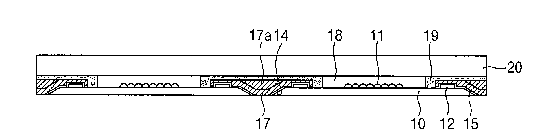
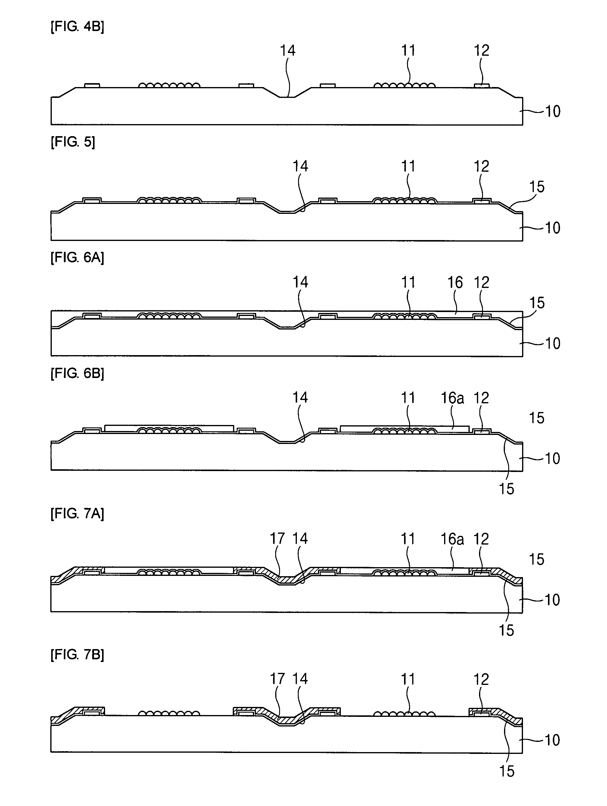
[0053]FIG. 2 is a cross-sectional view of a wafer level chip scale package of an image sensor according to a first embodiment of the present invention.

[0054]Referring to FIG. 2, the wafer level chip scale package includes a wafer 10 having inclined surfaces on both ends thereof, expansion pads 17, a support 19, and a glass 20. The wafer 10 includes an image sensor 11 and a pad 12 on the top surface thereof. The expansion pads 17 are formed on the inclined surfaces of the wafer 10 such that they are electrically connected to the pad 12. In addition, the expansion pads 17 are disposed in a straight line with respect to the bottom surface of the wafer 10. The support 19 is disposed on the expansion pads 17 to support both bottom surfaces of the glass 20 and has a height to define a space where an air cavity 18 can be formed. The glass 20 is disposed on the support 19 such that the air cavity 18 is formed above the wafer 10.

[0055]The wafer 10 is formed of silicon. An image sensor (micro...

second embodiment

[0100]A wafer level chip scale package of an image sensor according to a second embodiment of the present invention will be described below in detail with reference to FIG. 11. Detailed description about parts similar to those of the first embodiment will be omitted, but parts different from those of the second embodiment will be described below.

[0101]FIG. 11 is a cross-sectional view illustrating a wafer level chip scale package of an image sensor according to a second embodiment of the present invention.

[0102]Referring to FIG. 11, the wafer level chip scale package of the image sensor according to the second embodiment differs from that of the first embodiment in that a second expansion pad 17a is further formed on the expansion pad 17 formed conformally along the inclined surface of both ends of the wafer 10 so as to eliminate the surface height difference of the expansion pad 17.

[0103]In the first embodiment, the expansion pad 17 is formed conformally along the inclined surfaces...


PUM


Abstract

Provided are a wafer level chip scale package of an image sensor and a manufacturing method thereof. The wafer level chip scale package includes: a wafer including an image sensor and a pad on the top surface thereof and inclined surfaces on both ends thereof; expansion pads formed on the inclined surfaces of the wafer, including the pad, such that the expansion pads are electrically connected to the pad, a bottom surface of the expansion pads being on a straight line with respect to that of the wafer; a support formed on the expansion pads to support both bottom surfaces of a glass, the support having a height to provide a space where an air cavity is formed; and a glass disposed on the support to provide the air cavity over the wafer.

Description

CROSS-REFERENCE TO RELATED APPLICATIONS[0001]This application claims the benefit of Korean Patent Application No. 10-2006-0098468 filed with the Korea Industrial Property Office on Oct. 10, 2006, the disclosure of which is incorporated herein by reference.BACKGROUND OF THE INVENTION[0002]1. Field of the Invention[0003]The present invention relates to a wafer level chip scale package of an image sensor and a manufacturing method thereof. In the wafer level chip scale package of the image sensor, since expansion pads are provided instead of solder balls, a complicated process of forming solder balls can be omitted, thereby improving production capability. Since a glass is attached in a wafer level, defects caused by foreign particles can be minimized. Furthermore, miniaturization and slimness of the package can be realized.[0004]2. Description of the Related Art[0005]One of main trends in today's semiconductor industries is to miniaturize semiconductor devices as much as possible. The...

Claims


Application Information

Patent Timeline
Patent Type & Authority Patents(United States)
IPC IPC(8): H01L27/148H01L29/04H01L23/544
CPCH01L27/14618H01L31/0203H01L27/14683H01L27/14621H01L27/14627H01L2224/13H01L27/14685H01L31/0232H01L2224/05573H01L2224/05572H01L2924/00014H01L2224/0554H01L2224/05599H01L2224/0555H01L2224/0556H01L23/12
Inventor RYU, JIN MUNKIM, JUNG JINPARK, HYUNG KYU
Owner SAMSUNG ELECTRO MECHANICS CO LTD
Why Eureka
Try Eureka