Manufacturing method of optical low pass filter

A technology of low-pass filters and manufacturing methods, applied in optics, optical components, nonlinear optics, etc., can solve problems such as time-consuming, reduced production efficiency, and poor production efficiency

Inactive Publication Date: 2004-11-03
SEIKO EPSON CORP
View PDF1 Cites 7 Cited by
  • Summary
  • Abstract
  • Description
  • Claims
  • Application Information

AI Technical Summary

Problems solved by technology

[0009] However, although air bubbles do not remain when crimping is performed in a vacuum atmosphere, the manufacturing yield is improved, but there is a problem that it takes time to change from atmospheric pressure to vacuum, and the production efficiency is poor.
For this reason, the process under the vacuum atmosphere must be limited to a minimum so that the production efficiency will not be reduced.

Method used


Image

  • Manufacturing method of optical low pass filter
  • Manufacturing method of optical low pass filter
  • Manufacturing method of optical low pass filter

Examples


Embodiment Construction

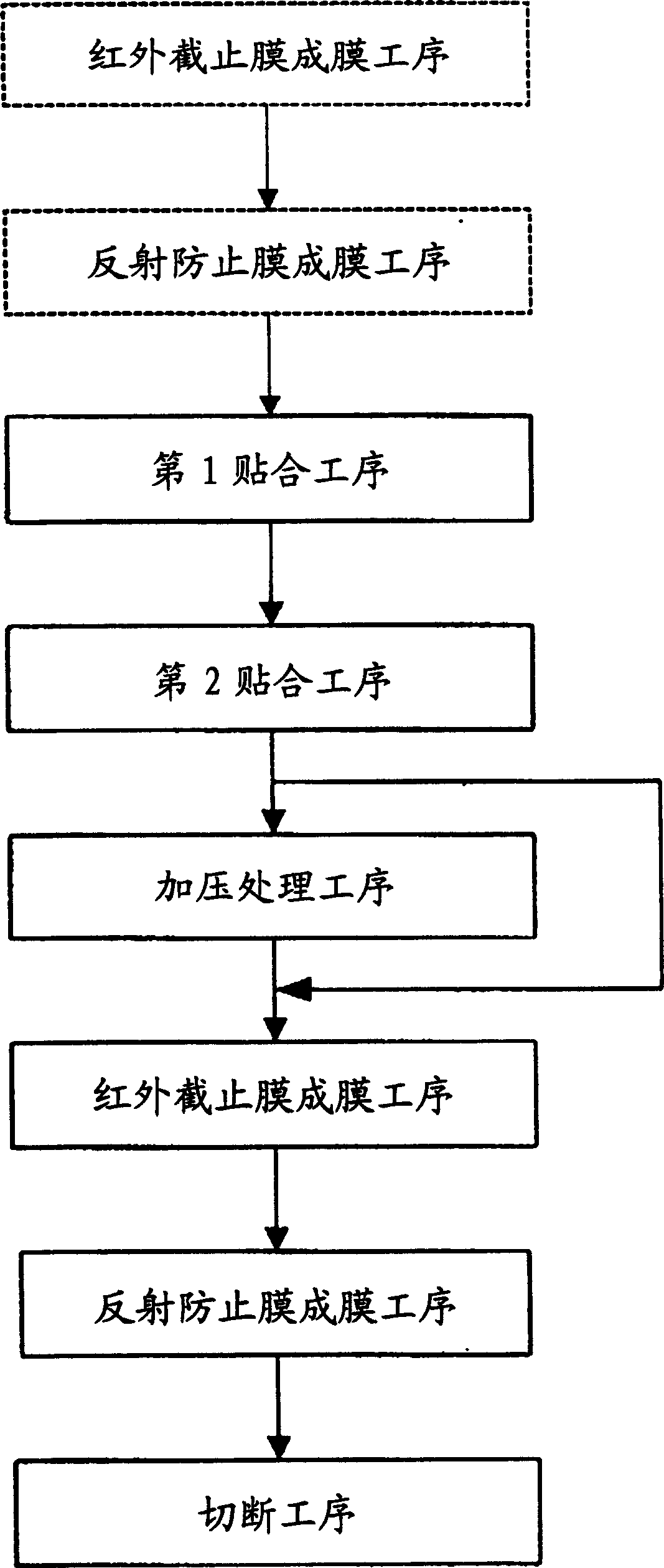
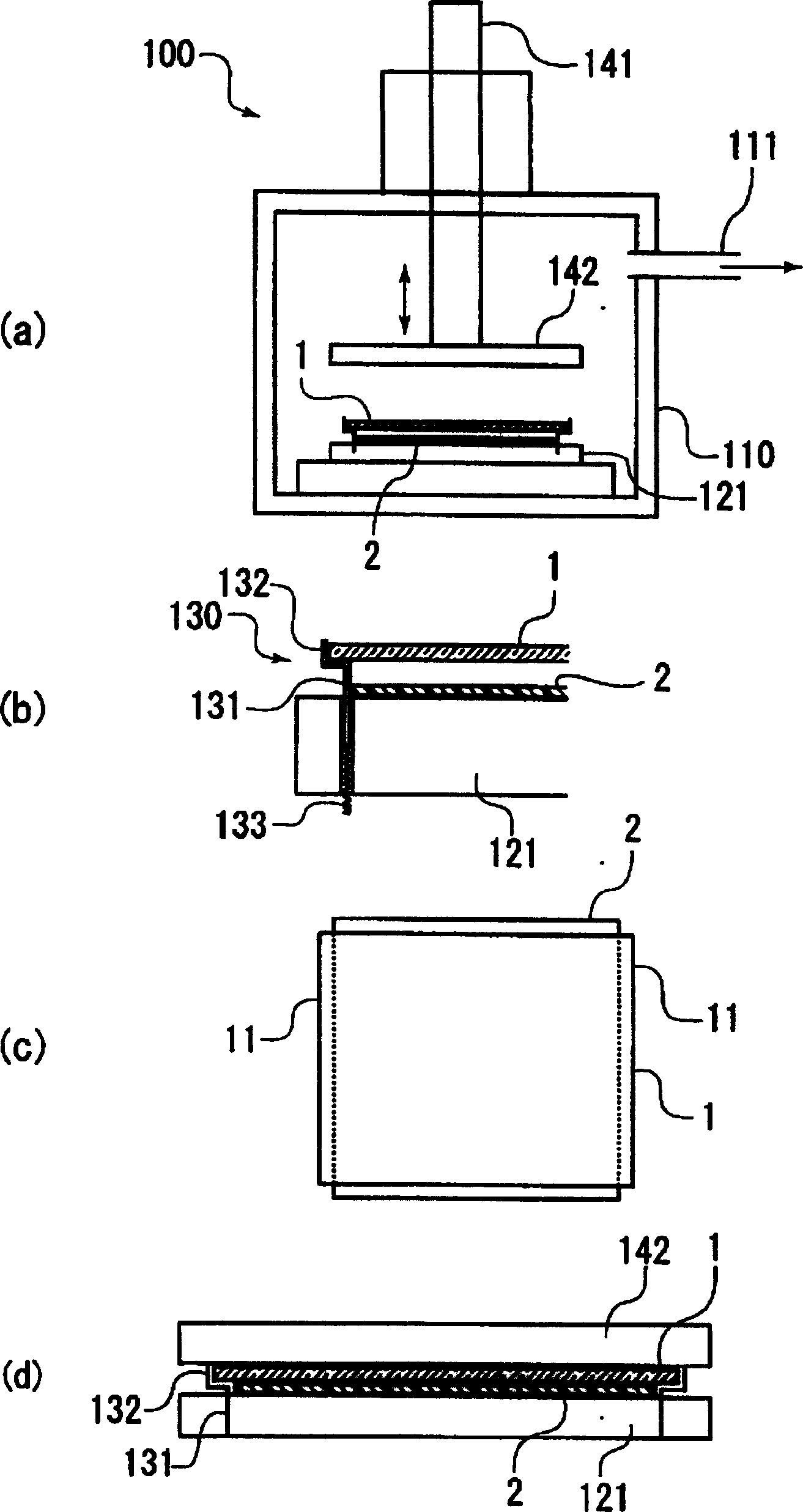
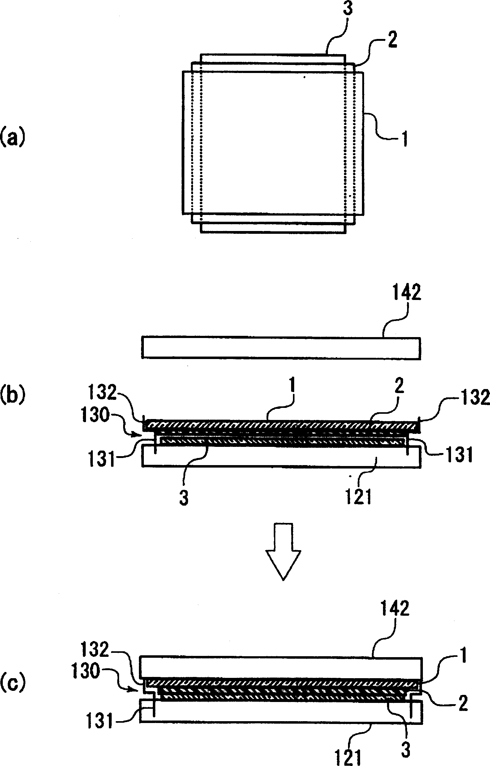
[0039] Hereinafter, embodiments of the method for manufacturing an optical low-pass filter of the present invention will be described, but the present invention is not limited to the following embodiments.

[0040] As an optical low-pass filter to be used in the method of manufacturing the optical low-pass filter of the present invention, a structure in which a 1 / 4 wavelength plate made of a polymer film is sandwiched between two birefringent plates can be cited. A 3-story structure of the vertical attachment type. A crystal plate having predetermined crystal planes is generally used as a birefringent plate. Examples of the polymer film constituting the 1 / 4 wavelength plate include uniaxially stretched plastic films. The 1 / 4 wavelength plate has the function of transforming the polarization state of incident light from linear polarization to circular polarization. A uniaxially stretched polymer film having a predetermined thickness has a characteristic that the birefringence...


PUM


Abstract

A manufacturing method of optical low-pass filtering lens with excellent production efficiency is provided, in which polymer thin film can be bonded on the dual-refraction plate with an excellent production yield and no bubble is occurred between polymer thin film and dual-refraction plate. In the manufacturing method of low-pass filtering lens, polymer thin film 2 is sandwiched between the first hard dual-refraction plate 1 and the second hard dual-refraction plate 3. The manufacturing method of low-pass filtering lens includes the followings: the first bonding process for bonding polymer thin film 2 on the first dual-refraction plate 1; and the second bonding process for pressing the second dual-refraction plate 3 on polymer thin film 3 in a vacuum environment after the first bonding process.

Description

technical field [0001] The present invention relates to the manufacturing method of optical low-pass filter (low pass filter), specifically relate to a kind of technology that can improve the manufacturing yield of optical low-pass filter, wherein this optical low-pass filter has the polymer film sandwiched between double Structures in the refraction sheet. Background technique [0002] Patent Document 1: JP-A-2003-29035 [0003] Imaging devices such as CCDs and CMOSs ​​are used in imaging devices such as digital still cameras and digital video cameras. The imaging element converts an optical image into an electrical signal by pixels arranged in a matrix at a predetermined pitch, and captures an image. In such an imaging device, if the spatial frequency of an optical image exceeds 1 / 2 of the sampling frequency determined by the arrangement pitch of pixels, spurious signals such as moire will be generated and image quality will be degraded. [0004] For this reason, in a g...

Claims


Application Information

Patent Timeline
IPC IPC(8): G02B5/30G02B1/10G02B27/46G02F1/03
CPCG02B1/11G02B5/281G02B5/30G02B27/46G02F1/0311
Inventor 原和弘有贺大助沟口健一
Owner SEIKO EPSON CORP
Why Eureka
Try Eureka