Method for mfg. connectors

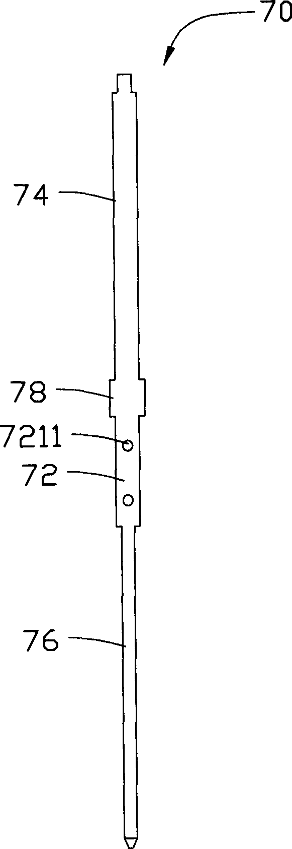
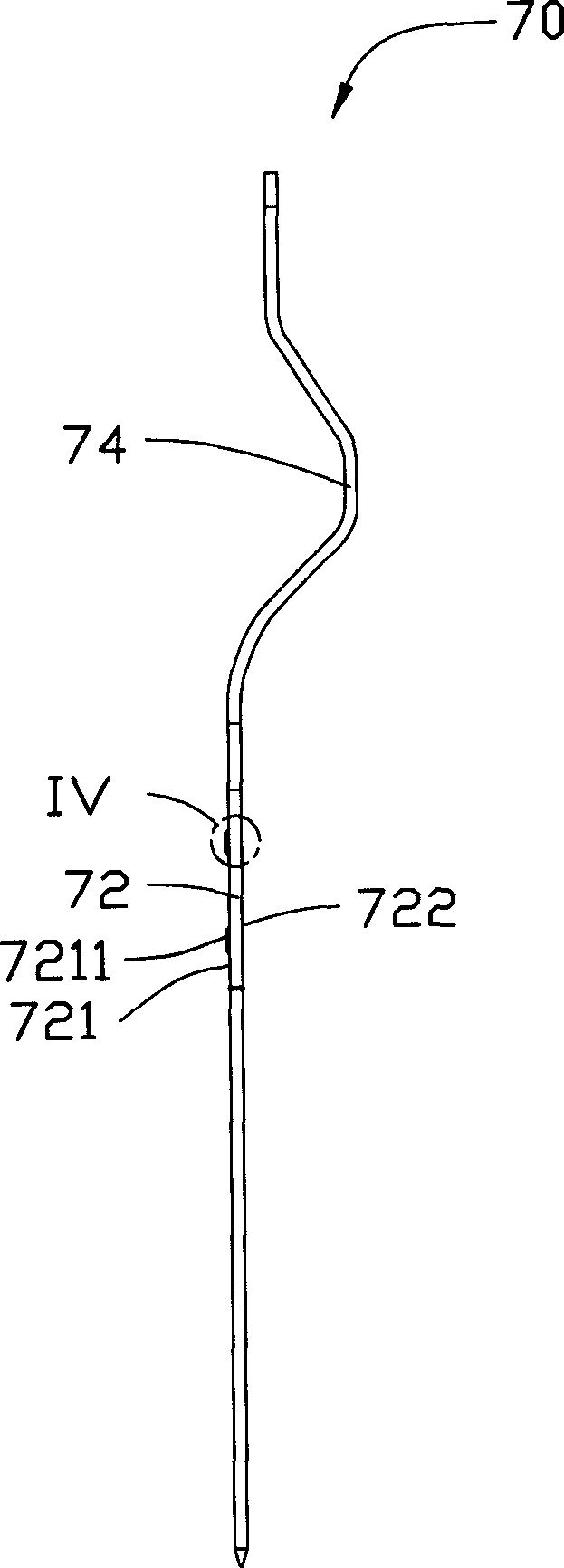
A manufacturing method and technology for electrical connectors, which are applied in the manufacture of contacts, the manufacture of contact boxes/bases, and the assembly/disassembly of contacts, can solve the deformation of the first mating surface 651, the recovery deformation of the bumps 7211, and the retention of Problems such as poor effect, to achieve the effect of increasing the holding force

Inactive Publication Date: 2005-03-09
FOXCONN (KUNSHAN) COMPUTER CONNECTOR CO LTD +1
View PDF0 Cites 1 Cited by
  • Summary
  • Abstract
  • Description
  • Claims
  • Application Information

AI Technical Summary

Problems solved by technology

However, because the thickness of the terminal 70 is small, usually 0.30mm, the diameter of the bump 7211 is usually no more than 0.6mm, and when punching the bump 7211, a concave hole 7222 of similar size will be formed on the second holding surface 722, so If the diameter of the bump 7211 is too large, its strength will be weak. When the insulating body 60 is stamped, the concave plastic due to plastic deformation pushes against the bump 7211, which will easily cause the bump 7211 to recover and deform, thereby making the terminal 70 The interference effect between the holding part 72 and the terminal hole 65 is not good
The width of the terminal 70 is usually more than 1.5 mm, which is much larger than the diameter of the bump 7211 of 0.6 mm. When punching the insulating body 60, it is necessary to press a larger area on the first mating surface 651 to the first holding surface 721, so for A certain stamping depth S1 (such as Figure 7 As shown), the amount of interference S2 generated by it is small, and the diameter of the bump 7211 is small, and the area where the pressed first mating surface 651 directly interferes with the bump 7211 is also small, and it can only be used with the plastic inner Part of the material is concave and deformed, and it is easy to deform the first mating surface 651 that interacts with the bump 7211, so that its holding effect is not good

Method used


Image

  • Method for mfg. connectors
  • Method for mfg. connectors
  • Method for mfg. connectors

Examples


Embodiment Construction

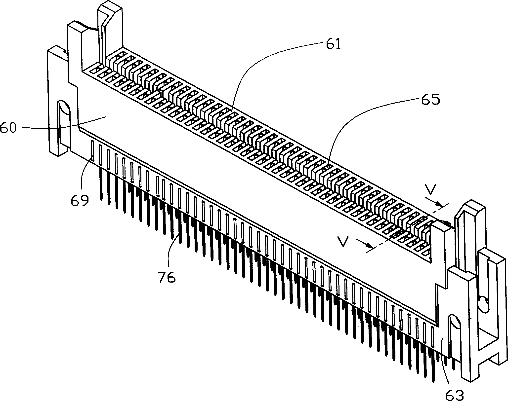
[0025] Please also refer to Figure 8~ Figure 12 The electrical connector 10 of the present invention is used to connect a sub-circuit board (not shown) to a circuit board (not shown), and includes a long and narrow insulating body 20 and a plurality of terminals 30 accommodated in the insulating body 20 .

[0026] The insulating body 20 has a mounting surface 22 for mounting on a circuit board, an inserting surface 21 opposite to the mounting surface 22 , and a first outer surface 23 perpendicular to the two surfaces. The first outer surface 23 is provided with a second outer surface 27 near the installation surface 22 for punching, and there is a concave step between the second outer surface 27 and the first outer surface 23 . The middle position of the insertion surface 21 is recessed with a groove 24 parallel to the long and narrow direction, and thus forms two side walls 26 and a bottom wall 28. On both sides of the groove 24, there is a penetrating installation surface 2...


PUM


Abstract

A manufacturing method for an electric connector includes: forming an insulation body having an outside face, multiple terminal holes through the body designed close to the outside face, forming multiple conduction terminals having a hold part fixing the terminals on the body, in which, at least a recess is set on the hold part, plugging the said terminals into the insulation body and plugging the hold part into the terminal hole and punching the outside face which is corresponding to the hold part of the terminals so as to enable the insulation body to turn concaved to form a proud in the recess part.

Description

【Technical field】 [0001] The invention relates to a manufacturing method of an electrical connector, in particular to a manufacturing method of an electrical connector capable of strengthening the holding force between an electrical connector terminal and an insulating body. 【Background technique】 [0002] It is well known in the industry that with the development of electrical connectors in the direction of miniaturization, high speed and stability, the insulating body and conductive terminals of electrical connectors are also developing in the direction of miniature and high density, which increases the difficulty of matching the electrical connector with its connected components. When the conductive terminal and the insulating body are not firmly fixed, it is easy to cause the terminal to loosen. Therefore, the industry uses a process of stamping the insulating body to plastically deform it to strengthen the terminal holding process, that is, stamping the insulating body ...

Claims


Application Information

Patent Timeline
Patent Type & Authority Applications(China)
IPC IPC(8): H01R43/16H01R43/18H01R43/20
Inventor 王佃刚林南宏
Owner FOXCONN (KUNSHAN) COMPUTER CONNECTOR CO LTD
Why Eureka
Try Eureka