Flat panel display and method for fabricating the same

A flat-panel display and area technology, applied in semiconductor/solid-state device manufacturing, static indicators, instruments, etc., can solve the difference between pixel TFT and drive circuit TFT, difficult adjustment, unit pixel and thin film transistor work of drive circuit different characteristics

Active Publication Date: 2005-05-25
SAMSUNG DISPLAY CO LTD
View PDF1 Cites 7 Cited by
  • Summary
  • Abstract
  • Description
  • Claims
  • Application Information

AI Technical Summary

Problems solved by technology

However, since pixel TFTs require different operating characteristics, pixel TFTs are different from driver circuit TFTs.
Therefore, when the thin film transistors of the unit pixel and the driving circuit are formed using the same crystallization method as described above, it is not easy to adjust the operating characteristics of the thin film transistors of the unit pixel and the driving circuit so as to be different from each other.

Method used


Image

  • Flat panel display and method for fabricating the same
  • Flat panel display and method for fabricating the same
  • Flat panel display and method for fabricating the same

Examples


Embodiment Construction

[0020] The present invention will now be described more fully with reference to the accompanying drawings, in which preferred embodiments of the invention are shown. However, the present invention can be carried out in different ways and is not limited to the embodiments described here. Rather, these embodiments are provided so that this disclosure will be thorough and complete, and will fully convey the scope of the invention to those skilled in the art. In the drawings, when a layer is described as being formed on another layer or a substrate, it means that the layer may be formed on another layer or a substrate, or may be interposed between this layer and another layer or a substrate. the third floor. Throughout the description, the same reference numerals refer to the same elements.

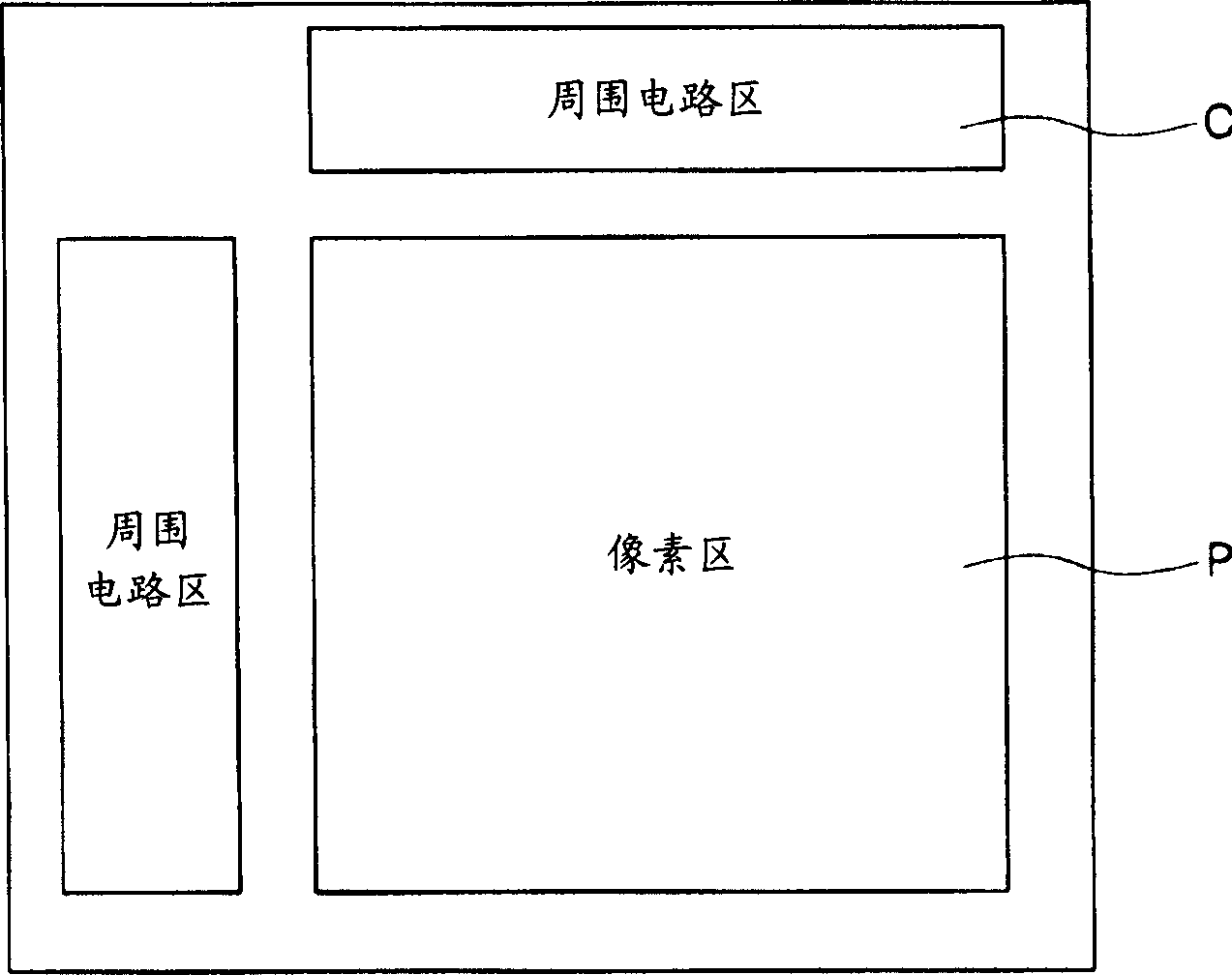
[0021] figure 1 A plan view of a flat panel display according to an embodiment of the present invention is shown.

[0022] refer to figure 1 , a pixel region P having a plurality of unit...


PUM


Abstract

Disclosed are a flat panel display and a manufacturing method thereof. In a flat panel display, a substrate includes a pixel area having a plurality of unit pixels, and a peripheral circuit area around the pixel area. The peripheral circuit area also includes a driving circuit for driving a plurality of unit pixels. At least one circuit thin film transistor is located in the peripheral circuit region and includes a first semiconductor layer crystallized by a sequential lateral solidification method. At least one pixel thin film transistor is located in the pixel area and includes a second semiconductor layer having a channel region crystallized by one of a metal-induced crystallization method or a metal-induced lateral crystallization method.

Description

[0001] This application claims the benefit of Korean Patent Application No. 2003-81257 filed on November 17, 2003, the entire content of which is hereby incorporated by reference. technical field [0002] The present invention generally relates to a flat panel display, and in particular, relates to a flat panel display with thin film transistors and a manufacturing method thereof. Background technique [0003] In recent years, flat panel displays such as Liquid Crystal Displays (LCD) or Organic Light Emitting Displays (OLED) have been active matrix types that produce high quality images. In an active matrix display, pixel electrodes and thin film transistors for controlling electrical signals applied to the pixel electrodes are located in each unit pixel of a pixel area. [0004] A thin film transistor includes a semiconductor layer, a gate insulating layer, and a gate electrode, and the semiconductor layer is usually a polysilicon layer whose electron mobility is about 100 ...

Claims


Application Information

Patent Timeline
Patent Type & Authority Applications(China)
IPC IPC(8): G02F1/136G02F1/1345G02F1/1362G09F9/30G09G3/00G09G3/36H01L21/00H01L21/77H01L21/84H01L27/12H01L27/32
CPCG02F1/13624H01L27/1229H01L27/1277H01L27/1285H10K59/12G02F1/136
Inventor 金勋李基龙徐晋旭
Owner SAMSUNG DISPLAY CO LTD
Why Eureka
Try Eureka