Semiconductor device

A semiconductor and conductive technology, applied in the field of ohmic connectivity components and semiconductor devices, can solve problems such as voltage difference and uneven operation, achieve uniform operation, suppress voltage drop, and ensure the number of units

Inactive Publication Date: 2005-06-08
SANYO ELECTRIC CO LTD
View PDF1 Cites 1 Cited by
  • Summary
  • Abstract
  • Description
  • Claims
  • Application Information

AI Technical Summary

Problems solved by technology

Due to this voltage difference, uneven operation in the device is caused

Method used


Image

  • Semiconductor device
  • Semiconductor device
  • Semiconductor device

Examples


Embodiment Construction

[0029] Below, refer to Figure 1 to Figure 9 A detailed description will be given of the semiconductor device and its manufacturing method of the present invention.

[0030] Example.

[0031] First, refer to Figure 1 ~ Figure 4 The semiconductor device of this embodiment will be described.

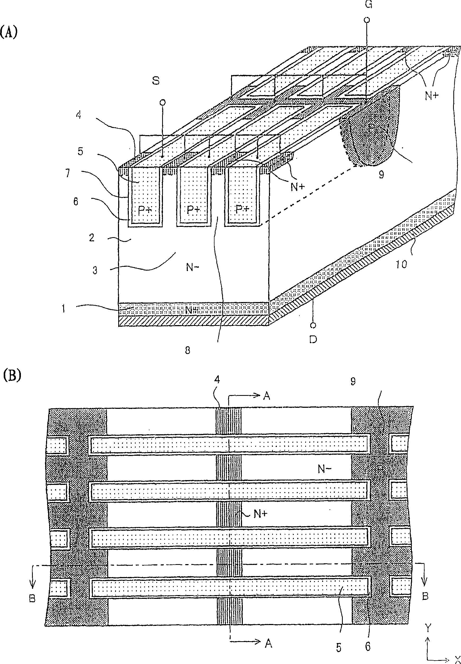
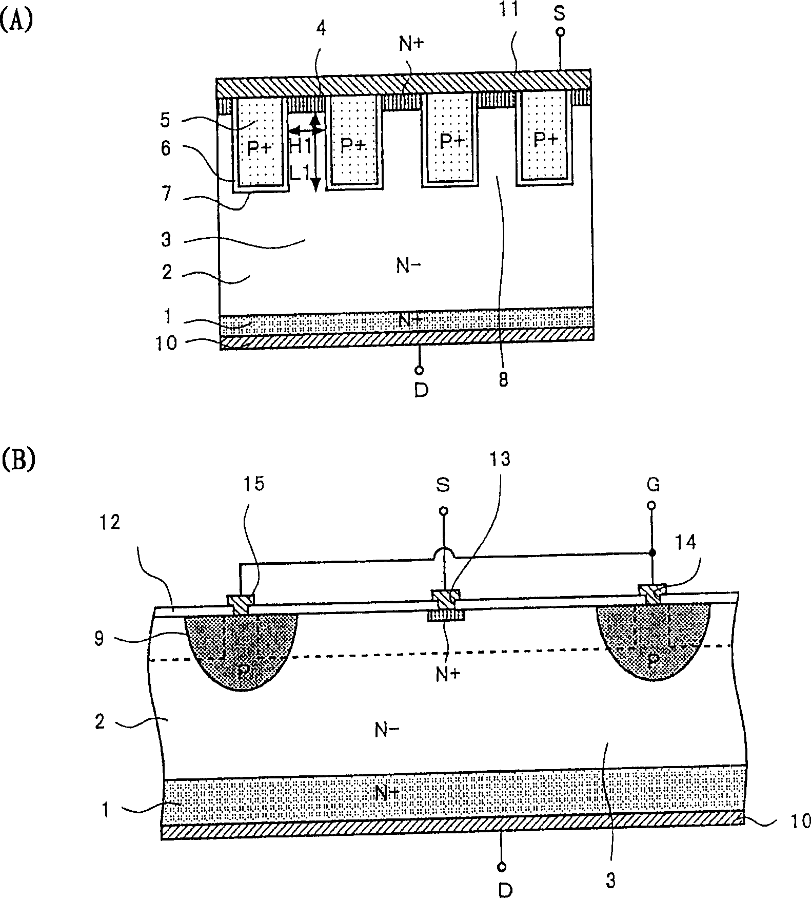
[0032] figure 1 (A) is a perspective view showing the structure of the semiconductor device of the present invention, figure 1 (B) is a top view showing the structure of the semiconductor device of the present invention. Such as figure 1 As shown in (A), an N-type epitaxial layer 2 is deposited on an N-type semiconductor substrate 1 . A plurality of grooves 7 are formed from the surface of the epitaxial layer 2 . The grooves 7 are arranged parallel to each other at equal intervals. The substrate 1 is used as a drain extraction region, and the epitaxial layer 2 is mainly used as a drain region 3 . In addition, the side walls of the groove 7 are etched substantially perpendicula...


PUM


Abstract

A semiconductor device. In the conventional semiconductor device, there is a problem that the wiring width of the main wiring part through which the main current flows is narrow and uniform, and the cells in the device do not operate uniformly due to the voltage drop of the main wiring part. . In the semiconductor device of the present invention, the wiring width W1 of the one end 241 of the main wiring portion 24 through which the main current flows is set wider than the wiring width of the other end 242 of the main wiring portion 24 . The wiring width of the main wiring portion 24 gradually narrows from one end 241 to the other end 242 . Accordingly, it is possible to reduce the drive voltage difference between a cell located near the electrode pad portion 22 through which the main current flows and a cell located far away. As a result, the present invention suppresses the voltage drop of the main wiring portion 24 and realizes uniform operation of the cells in the element.

Description

technical field [0001] The semiconductor device of the present invention relates to an element for improving ohmic connectivity between a fixed-potential insulating electrode and a source region formed of polysilicon, and a metal layer. Background technique [0002] A conventional lateral insulated gate transistor has disclosed a structure in which an emitter electrode and a gate electrode are arranged in a zigzag shape on the main surface of a semiconductor layer. Furthermore, the resistance per unit length in the longitudinal direction is equal at these sawtooth portions, thereby forming a structure that prevents local concentration of ON current flowing from the collector to the emitter (for example, refer to Patent Document 1). [0003] A conventional transistor has disclosed a structure having a zigzag base and an emitter (see, for example, Non-Patent Document 1). [0004] refer to Figure 10 and Figure 11 , shows an example of a conventional semiconductor device str...

Claims


Application Information

Patent Timeline
Patent Type & Authority Applications(China)
IPC IPC(8): H01L21/28H01L29/417H01L29/423H01L29/49H01L29/76H01L29/78H01L29/80
CPCH01L29/41741H01L29/4236H01L29/4238H01L29/4916H01L29/7828H01L29/80
Inventor 吉田哲哉冈田哲也斋藤洋明村井成行冈田喜久雄
Owner SANYO ELECTRIC CO LTD
Why Eureka
Try Eureka