

Multifunctional nano research and development platform
A development platform and multi-functional technology, applied in the field of research and development systems, can solve problems such as no probe head
- Summary
- Abstract
- Description
- Claims
- Application Information
AI Technical Summary
Problems solved by technology
Method used
Image

Examples
Embodiment 1
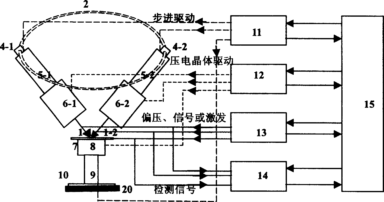
[0040] figure 2 A practical scheme of the platform of the present invention enabling three probes and samples to work in the same microarea is shown. In this scheme, the probe positioning drive system and the sample positioning drive system are respectively composed of their own positioning track system, stepping drive system and piezoelectric crystal drive system (see attached image 3 ) consists of three parts. The position of the sample is determined by the position of the sample stage on which it is placed.
[0041] The probe orientation track system in this scheme is a centripetal track system, including:
[0042] (1), determine the probe longitude rail 0 of the probe longitude;
[0043] (2), the probe latitude guide rails 2-1, 2-2, 2-3 for locking the longitude of the probe and determining the latitude of the probe, each guide rail is an arc greater than 1 / 4 circumference;
[0044] (3), the positioning rotating shaft 2-0 of the probe latitude guide rail.
[0045] T...
Embodiment 2
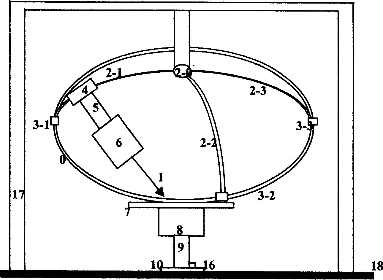
[0060] The research and development platform of the present invention docks two probe tips to form an example of a one-dimensional nano-junction (see attached Figure 4 ).
[0061] 1. In this example, the tip of the probe is an exposed surface of a nano-microstructure, which can form a nano-research object or a part of the structure. On the basis that the tip of the probe 1-1 and 1-2 are opposite to each other by the probe stepping drive system (see attached Figure 4 ), the system workstation 15 controls the platform piezoelectric crystal driving power supply 12, so that the needle tips of the two heterogeneous probes 1-1, 1-2 (N-type and P-type) are relatively close to produce a tunnel effect, and then scan each other , to determine the atomic arrangement structure of the surface of each other. The system workstation 15 selects and makes appropriate surface structures close to each other by controlling the stepping drivers 5-1 and 5-2 of the rotation angle until "contact" ...
Embodiment 3
[0066] An example of the interaction between two probes and nanowires illustrates how the platform forms a multifunctional "nanomanipulator" for microstructure processing, manipulation, assembly, and control (see attached Figure 5 ).
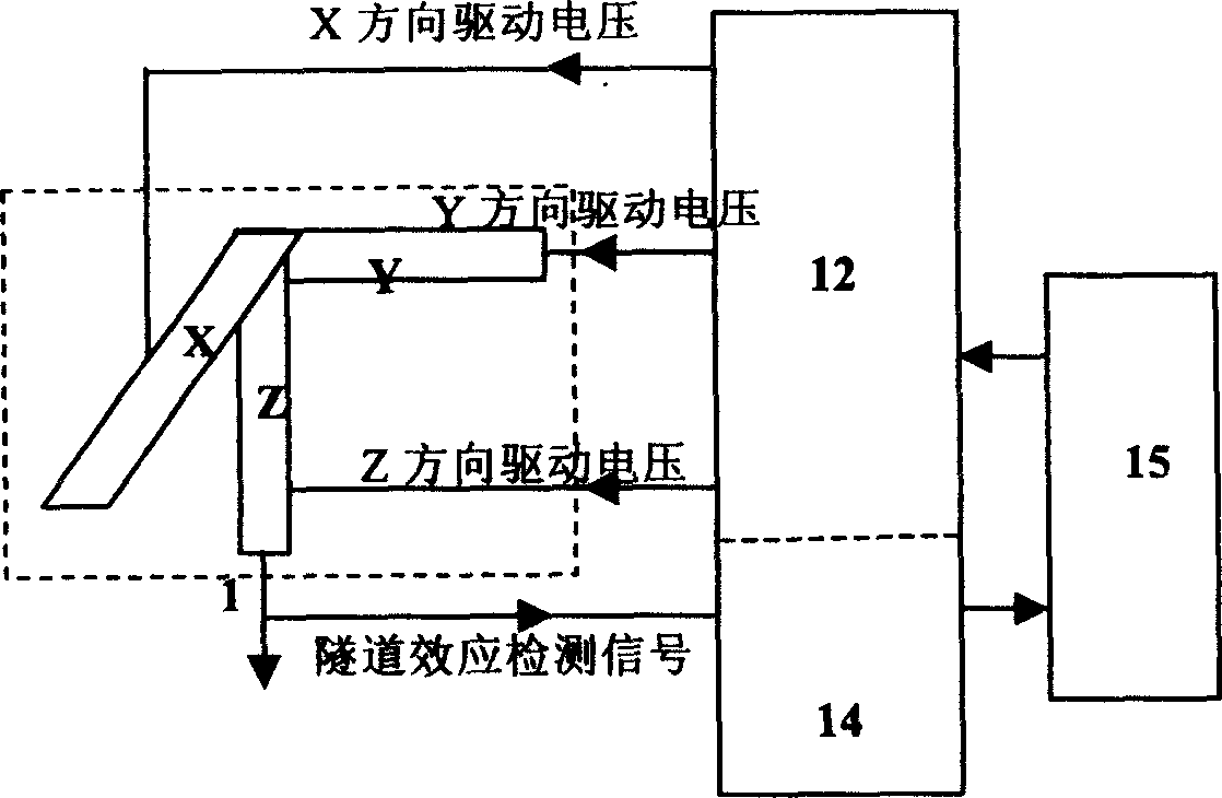
[0067] 1. The system workstation 15 drives the stepping drivers 3-1, 4-1, 5-1 of the probe 1-1 and the stepping drivers 9, 16 of the sample stage through the stepping drive power supply 11 of the control platform, so that the probe 1-1 Approach different parts of the nanowire 19 on the sample substrate; the workstation 15 instructs the platform signal generation system 13 to generate a bias voltage to be applied between the sample and the probe, and at the same time instructs the platform signal acquisition and amplification system 14 to collect the gap between the sample and the probe. tunnel current, according to the size of the detected tunnel current, a feedback control command is sent to the piezoelectric crystal drive power supply 12 to d...
PUM
 Abstract
Description
Claims
Application Information