Organic electroluminescent device and electronic apparatus

An electroluminescence device and electroluminescence technology, which are applied to electroluminescence light sources, instruments, electric light sources, etc., can solve the problems of only determining the position of the substrate surface direction, shortening life, and reducing conductivity.

Inactive Publication Date: 2005-09-07
SEIKO EPSON CORP
View PDF1 Cites 15 Cited by
  • Summary
  • Abstract
  • Description
  • Claims
  • Application Information

AI Technical Summary

Problems solved by technology

In the organic EL element constituting such an organic EL display device, there are problems in that the electro-optical material forming the light-emitting layer is affected by oxygen or moisture, and the conductivity is reduced by the influence of oxygen or moisture. shortened lifespan
However, in a top emission type organic EL device that emits light from the opposite substrate side, since the display light passes through the interior of the above-mentioned sealing structure, the adhesive resin has a great influence on the characteristics of t

Method used


Image

  • Organic electroluminescent device and electronic apparatus
  • Organic electroluminescent device and electronic apparatus
  • Organic electroluminescent device and electronic apparatus

Examples


no. 3 Embodiment approach

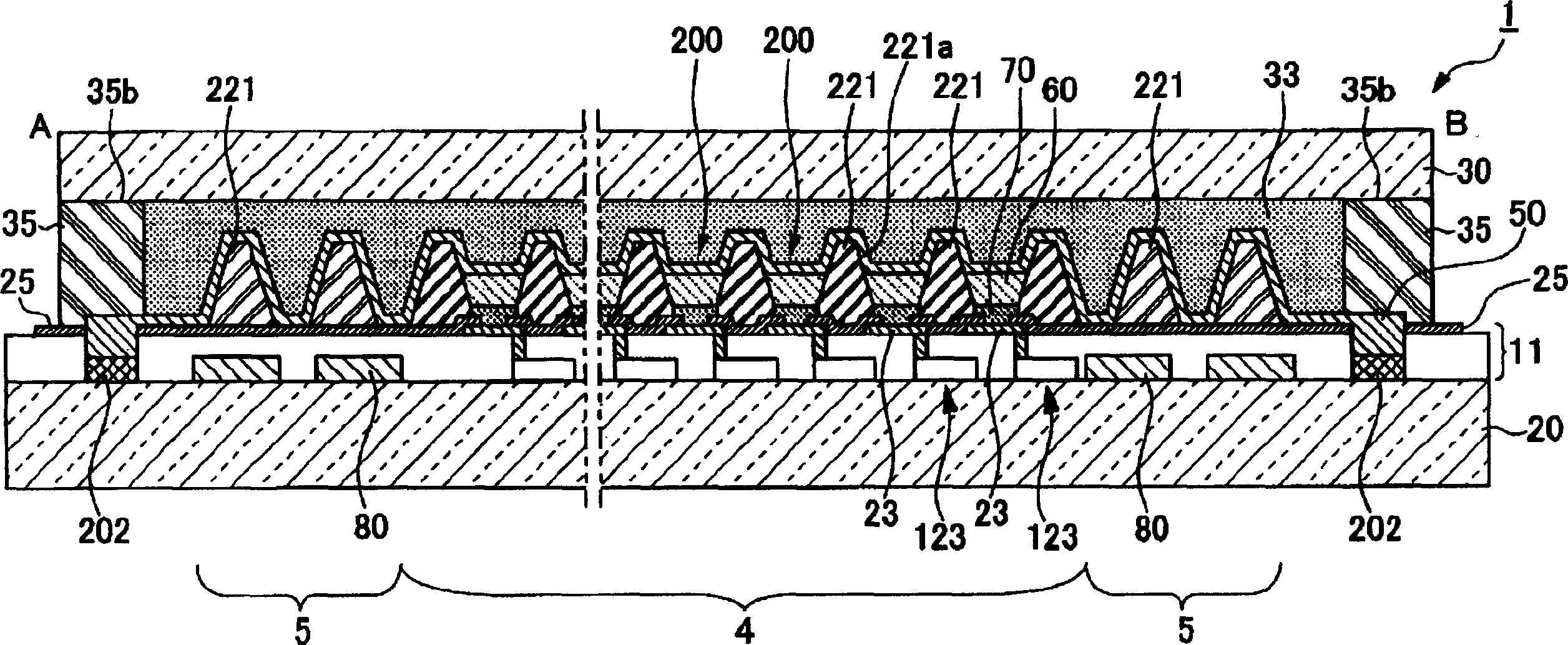
[0089] Refer to the following Figure 7A third embodiment of the present invention will be described. Figure 7 It is a partial cross-sectional configuration diagram showing an enlarged side end portion of the organic EL device according to the present embodiment. The organic EL device of this embodiment is characterized in that the contact portion of the protective substrate 30 and the spacer 35 is provided in an embedded structure, and other configurations are the same as those of the first embodiment above. therefore, Figure 7 Among the constituent elements shown, pay Figure 1 to Figure 5 Components with the same symbols are the same components.

[0090] Such as Figure 7 As shown, in the organic EL device of this embodiment, the outer end portion of the protective substrate 30 on the element substrate 20 side is provided with a notch portion 30a, and the inner side of the upper end portion of the spacer 35 erected on the element substrate 20 is opposite to the The c...

no. 4 Embodiment approach

[0092] Refer to the following Figure 8 A fourth embodiment of the present invention will be described. Figure 8 It is an enlarged partial cross-sectional configuration diagram of the outer end portion of the organic EL device according to the present embodiment. The organic EL device of this embodiment is characterized in that the contact portion between the protective substrate 30 and the spacer 35 is provided in an embedded structure, and other configurations are the same as those of the first embodiment above. therefore, Figure 8 Among the constituent elements shown, pay Figure 1 to Figure 5 Components with the same symbols in are the same components.

[0093] Such as Figure 8 As shown, in the organic EL device of the present embodiment, a notch 35c is provided inside the upper end portion of the spacer 35 standing upright on the element substrate 20 to protect the edge portion of the element substrate 20 side of the substrate 30 against the The cutout portion 35c...


PUM


Abstract

The objective of the invention is to provide an organic electroluminescent device having a sealing structure formed by arranging an adhesion layer and a protection substrate on a light emitting element, capable of taking out a good display light from protection plate side, and preferably, capable of obtaining excellent reliability even at the peripheral area where a connection terminal or the like is arranged. The organic electroluminescent device has an element substrate 20 on one face side of which, organic EL elements 200 are formed, and a protection substrate 30 adhered to the element substrate 20 through an adhesion layer 33 arranged on the organic EL elements. A separation member 35 holding both substrates 20, 30 with a prescribed distance is arranged between the substrates 20, 30.

Description

technical field [0001] The present invention relates to organic electroluminescent devices and electronic instruments. Background technique [0002] Conventionally, in an electro-optical device such as an organic electroluminescent (hereinafter referred to as organic EL) display device, it is known that a light-emitting layer formed of an electro-optical material such as an anode, a hole injection layer, and an EL material, and a cathode are stacked on a substrate. Structure. In the organic EL element constituting such an organic EL display device, there are problems that the electro-optical material forming the light-emitting layer is deteriorated by the influence of oxygen or moisture, and the conductivity of the cathode is reduced by the influence of oxygen or moisture. shortened lifespan. [0003] As a technique for solving such problems, it is conventionally known to form a light-emitting element on a support substrate, bond the surface of the support substrate on the...

Claims


Application Information

Patent Timeline
IPC IPC(8): H05B33/04G02F1/1339G09F9/30H01L27/32H01L51/50H01L51/52H05B33/02H05B33/06H05B33/10H05B33/12H05B33/14
CPCH01L27/3244H01L51/5237H10K59/12H10K50/8428H10K50/8426H10K71/70H05B33/04
Inventor 下神耕造林建二
Owner SEIKO EPSON CORP
Why Eureka
Try Eureka