Test terminal negation circuit

A technology for testing terminals and circuits, applied in circuits, measuring electricity, measuring electrical variables, etc.

Active Publication Date: 2005-10-05
知识产权I公司
View PDF0 Cites 0 Cited by
  • Summary
  • Abstract
  • Description
  • Claims
  • Application Information

AI Technical Summary

Problems solved by technology

[0005] In addition, although Japanese Unexamined Patent Publication No. 2002-269523 discloses a method of erasing information stored in a nonvolatile memory in an IC card when erroneous activation of the test mode is detected, in this method , additional circuitry must be provided to detect false activation of the test mode

Method used


Image

  • Test terminal negation circuit
  • Test terminal negation circuit
  • Test terminal negation circuit

Examples


Embodiment Construction

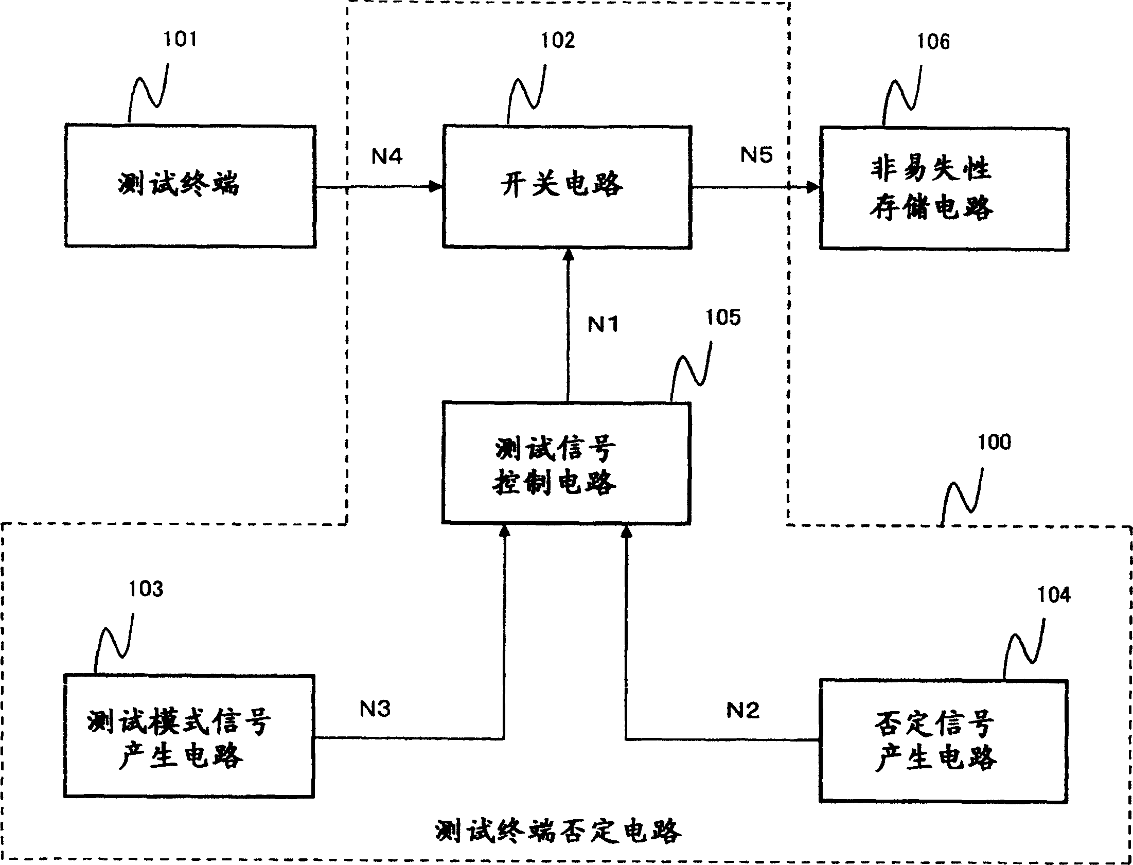
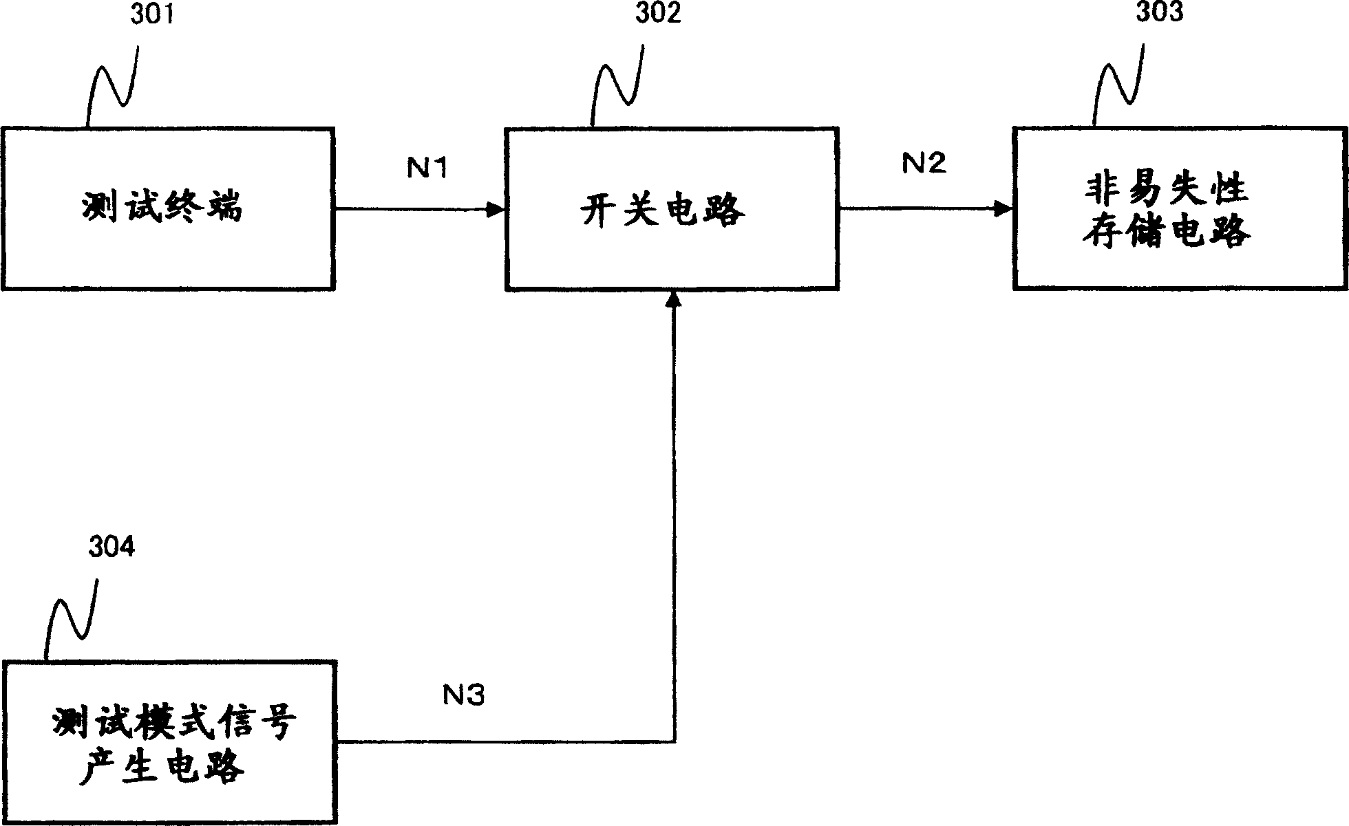
[0019] Embodiments of the present invention will be described with reference to the drawings. figure 1 is a circuit diagram showing an embodiment of a test terminal negation circuit according to the present invention (hereinafter sometimes referred to as "circuit of the present invention"). Such as figure 1 As shown in , the circuit 100 of the present invention includes a switch circuit 102 , a test mode signal generation circuit 103 , a negative signal generation circuit 104 , and a test signal control circuit 105 .

[0020] The switch circuit 102 receives the test signal from the test terminal 101 and relies on the level of the output node N1 of the test signal control circuit 105 to output it to the non-volatile storage circuit 106 in its affirmed state or a predetermined negated state , the nonvolatile storage circuit 106 is the object circuit to be tested. For example, the switching circuit 102 includes a CMOS transmission gate or the like.

[0021] The test mode signa...


PUM


Abstract

A test terminal negation circuit (100) comprises a switch circuit (102) receiving a test signal from a test terminal (101) and outputs it in an asserted state as it is or in a predetermined negated state to a test object circuit (106), a test signal control circuit (105) which controls an output signal of the switch circuit (102) to be asserted or negated, a test mode signal generation circuit (103) which generates a test mode signal which asserts the output signal of the switch circuit (102), and a negating signal generation circuit (104) which can output a negating signal for forcing the output signal of the switch circuit (102) into negated state and comprises an electrically rewritable nonvolatile memory element. When the test signal control circuit (105) receives the negating signal, it does not assert the output signal of the switch circuit (102) even it receives the test mode signal.

Description

technical field [0001] The present invention relates to a test terminal negation circuit in which a test signal cannot be received from a test terminal using a non-volatile memory after a test is completed. Background technique [0002] Currently, an IC card mounted with a nonvolatile memory is in the spotlight. Although IC card terminals are standardized in ISO7816, there are many kinds of test terminals to help testing. In normal operation, since data is exchanged by authenticating reader / writer etc. and encrypting data, confidential data will not be leaked. [0003] As a conventional technique, there is a method of turning on a switch circuit to output a test signal from a test terminal to a circuit under test by activating an output of a test mode signal generating circuit when the test terminal is used, and in the method The circuit configuration is shown in FIG. 3 (for example, refer to Japanese Unexamined Patent Publication No. 2002-269523). Referring to FIG. 3 , e...

Claims


Application Information

Patent Timeline
IPC IPC(8): G01R31/28G01R31/317G01R31/3185G06F21/60G06F21/79G06K19/07G11C29/02
CPCG01R31/31701H01L22/00
Inventor 福原周郎
Owner 知识产权I公司
Why Eureka
Try Eureka