Supercharge Your Innovation With Domain-Expert AI Agents!

Method for producing semiconductor device

A manufacturing method and semiconductor technology, applied in semiconductor/solid-state device manufacturing, semiconductor devices, electrical components, etc., can solve the problems of silicon interface influence, gate oxide film reliability, transistor performance deterioration, etc., and achieve the effect of stabilizing charge and interface level

Inactive Publication Date: 2005-10-19
ELPIDA MEMORY INC
View PDF0 Cites 2 Cited by
  • Summary
  • Abstract
  • Description
  • Claims
  • Application Information

AI Technical Summary

Problems solved by technology

[0006] However, in the related art described above, nitrogen contained in the oxynitride film acts as a positive charge, adversely affecting the silicon interface
In addition, even if the inner wall of the trench is oxynitrided, the formation of the gate oxide film is suppressed, therefore, the film has a thin portion
Therefore, the related art undesirably causes undesired deterioration of the reliability of the gate oxide film and the performance of the transistor because the gate oxide film has a thin portion and the electric field is concentrated

Method used


Image

  • Method for producing semiconductor device
  • Method for producing semiconductor device
  • Method for producing semiconductor device

Examples


Embodiment Construction

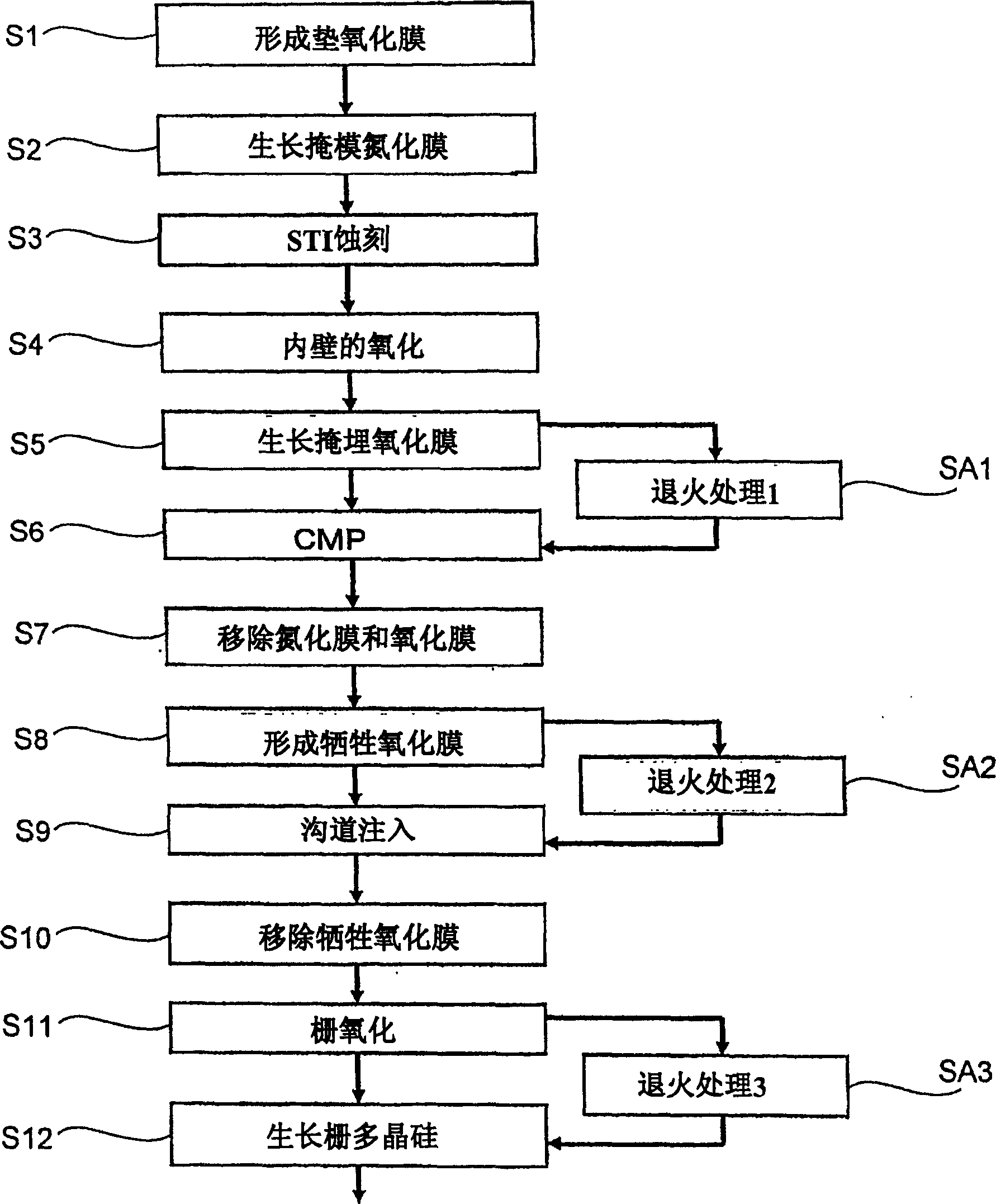
[0027] A method of manufacturing a semiconductor device according to the present invention will now be described with reference to the drawings.

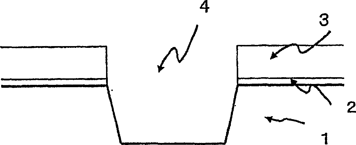
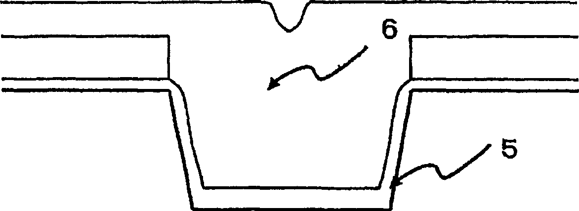
[0028] First, a pad oxide film 2 with a thickness of 9 nm and a nitride film 3 with a thickness of 140 nm are formed on the main surface of a silicon substrate 1, as figure 1 Steps S1 and S2 of and Figure 2A shown. Then, the nitride film 3 and the pad oxide film 2 are etched by photolithography, and the silicon substrate 1 is etched to form a trench 4, such as figure 1 Step S3 and Figure 2A shown. The inner wall of trench 4 is oxidized to form inner wall oxide film 5 with a thickness of 20 nm. Then fill the trench 4 with the buried oxide film 6, as figure 1 Steps S4 and S5 of and Figure 2B shown.

[0029] The buried oxide film 6 is polished by chemical mechanical polishing (CMP) until the nitride film 3 is exposed, such as figure 1 Step S6 of , and thus form a flat surface. Then remove the nitride film 3 and the pad oxid...


PUM


Abstract

A method for producing a semiconductor device includes the steps of forming a trench for device isolation on a silicon substrate; and annealing the silicon substrate in an atmosphere containing a noble gas at any step after the growth of a buried oxide film until the growth of a gate polysilicon.

Description

technical field [0001] The present invention relates to a method of manufacturing a semiconductor device, and more particularly to a method of manufacturing a semiconductor device without deteriorating device characteristics by improving the reliability of a gate oxide film at the boundary between a trench isolation region and an active region. Background technique [0002] In recent years, there has been an increasing demand for larger-scale, higher-speed semiconductor devices. In order to meet this demand, STI (Shallow Trench Isolation) has been used as a method of isolating devices. In STI, an insulating film is buried in a trench to achieve isolation. Therefore, this method produces no bird's beak effect compared with LOCOS (Local Oxidation of Silicon), and is suitable for obtaining a high degree of integration. [0003] However, in STI, a quadrilateral STI corner is formed at the boundary between the active region, the main silicon surface, and the isolation region, t...

Claims


Application Information

Patent Timeline
Patent Type & Authority Applications(China)
IPC IPC(8): H01L21/76H01L21/28H01L21/316H01L21/324H01L21/762H01L29/78
CPCH01L21/76224H01L21/28185H01L21/28238
Inventor 大桥拓夫诹访刚久保田大志
Owner ELPIDA MEMORY INC
Features
  • R&D
  • Intellectual Property
  • Life Sciences
  • Materials
  • Tech Scout
  • Unparalleled Data Quality
  • Higher Quality Content
  • 60% Fewer Hallucinations
Learn More