Eureka AIR delivers breakthrough ideas for toughest innovation challenges, trusted by R&D personnel around the world.

Method for realizing Fanout design in PCB

A technology of implementation method and design information, applied in the direction of multi-layer circuit manufacturing, etc., can solve the problems of poor PCB design consistency, inconvenient maintenance and management, low efficiency of Fanout design, etc., and achieve the effect of improving efficiency and flexible Fanout design.

Inactive Publication Date: 2005-12-21
HUAWEI TECH CO LTD
View PDF0 Cites 1 Cited by
  • Summary
  • Abstract
  • Description
  • Claims
  • Application Information

AI Technical Summary

Problems solved by technology

[0004] However, the implementation of the Fanout design involved in the current PCB design is mainly done by the PCB engineer manually, which makes it necessary for the PCB design engineer to manually complete the corresponding Fanout design one by one even for the same package device, and, for a PCB design The Fanout design form designed by the engineer, when the engineer designs another PCB, the original Fanout design form can meet the requirements, and it also needs to be redesigned. Therefore, there is no Fanout design sharing mechanism that will lead to PCB design. The efficiency of the Fanout design is low, which in turn leads to a significant reduction in the efficiency of the entire PCB design
[0005] Moreover, in the specific design process, the design results of different engineers will be different; in this way, on the one hand, the consistency of PCB design will be poor, which is not convenient for subsequent maintenance and management; Experiences are different, which leads to the advantages and disadvantages of the above-mentioned various design results. For the best Fanout design form, it cannot be shared among the same Fanout design environments of different PCB design engineers, resulting in Unable to get optimal Fanout design

Method used

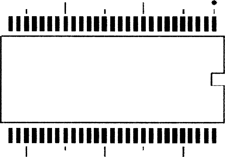
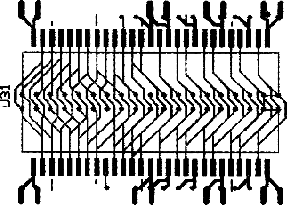

Image

  • Method for realizing Fanout design in PCB
  • Method for realizing Fanout design in PCB
  • Method for realizing Fanout design in PCB

Examples


Embodiment Construction

[0037] The core of the present invention is to save the Fanout design for each packaged device in the PCB design, so that it can be reused in the subsequent PCB design process, or when the Fanout design for the packaged device is needed again in other PCB design processes. The original Fanout design information, thereby effectively improving the efficiency of PCB design, especially improving the efficiency of Fanout design.

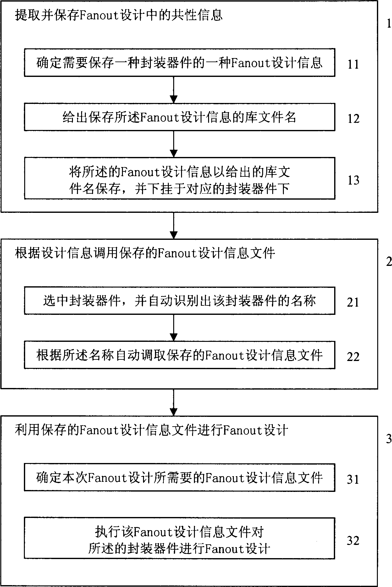
[0038] Below in conjunction with accompanying drawing, the implementation method of Fanout design in the PCB design of the present invention is described in detail, as figure 1 As shown, the method specifically includes the following steps:

[0039] Step 1: In order to reuse the design information in the Fanout design process, extract the common information in the Fanout design and save it;

[0040] Described step 1 further comprises the following steps:

[0041] Step 11: Determine that a fanout design information of a packaged device needs to be saved;...


PUM


Abstract

First, the method picks up and saves general information in Fanout design. Then, in procedure of Fanout design, using saved information file in Fanout design carries out Fanout design in PCB design. The invention reuses excellent Fanout design, i.e. information of Fanout design is shared so as to raise efficiency of design, also obtain better result of Fanout design. In the invention, one encapsulation part is corresponding to multiple forms of Fanout design. Thus, Fanout design for one kind of encapsulation part is more flexible.

Description

technical field [0001] The invention relates to the field of PCB (printed circuit board) design, in particular to a method for realizing Fanout (fan-out) design in PCB design. Background technique [0002] In the current PCB design, Fanout design is a job after the PCB layout is completed and before wiring. It mainly occurs in high-level (greater than 2 layers) PCB designs where surface mount devices are present. The purpose is to connect the SMD (Surface Mount Device) pads that only existed on the surface layer to the inner layer by laying a line and via holes, so that the inner layer wiring design in the later stage does not need to pay attention to the SMD pads on the surface layer. The line that originally needs to be connected to the SMD pad can be directly connected to the via hole from the Fanout of the SMD pad, and there is no need to add a via hole, thus avoiding the impact on other layers. Therefore, Fanout design is an important link between layout and wiring in...

Claims


Application Information

Patent Timeline
Patent Type & Authority Applications(China)
IPC IPC(8): H05K3/46
Inventor 李广生
Owner HUAWEI TECH CO LTD
Why Eureka
Eureka Blog
Learn More