Method of fabricating PCB including embedded passive chip

A passive chip and embedded technology, applied in the fields of printed circuit manufacturing, final product manufacturing, containing printed electrical components, etc., can solve problems such as difficult handling, long distance of integrated circuits, inability to form circuits with capacitor chips, etc.

Inactive Publication Date: 2006-01-18
SAMSUNG ELECTRO MECHANICS CO LTD
View PDF1 Cites 12 Cited by
  • Summary
  • Abstract
  • Description
  • Claims
  • Application Information

AI Technical Summary

Problems solved by technology

[0017] However, the problem with this method is that since the capacitor chip is mounted on the core layer, the distance between the capacitor chip and the integrated circuit (IC) mounted on the surface of the core layer is too large
In addition, since the capacitor chip cannot be mounted in the core layer until the via hole through the core layer is formed, an additional hole-forming process is required, and even if the capacitor chip is mounted on the via hole, it cannot be mounted on the capacitor chip. Circuits are formed on the upper and lower sides of the chip
[0018] Also, the process of mounting the capacitor chip in the through hole of the core layer is not easy to handle since the capacitor chip may fall from the core layer

Method used


Image

  • Method of fabricating PCB including embedded passive chip
  • Method of fabricating PCB including embedded passive chip
  • Method of fabricating PCB including embedded passive chip

Examples


no. 1 approach

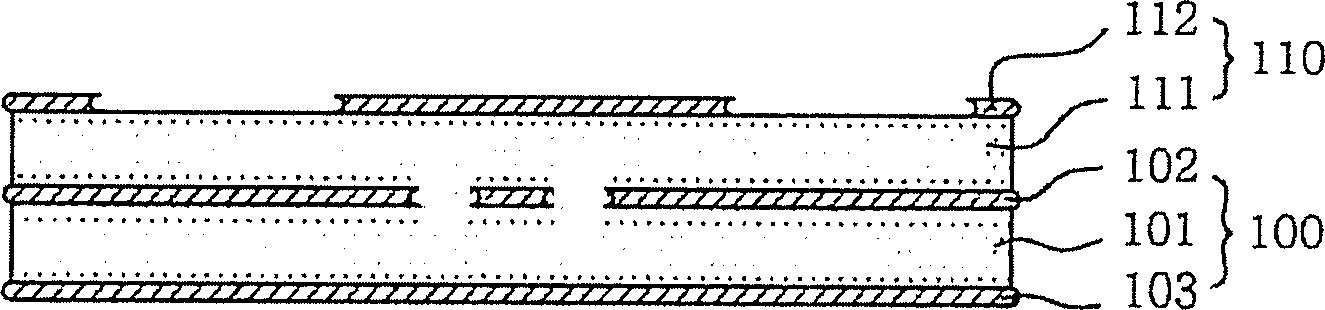
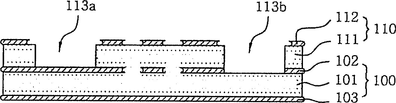
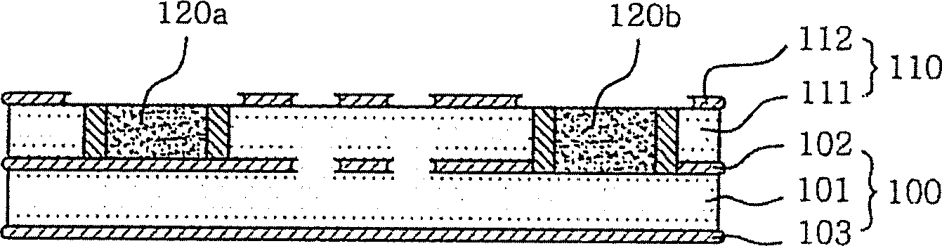
[0040] Figures 1a to 1e is a cross-sectional view illustrating a method of manufacturing a PCB containing embedded passive chips according to a first embodiment of the present invention

[0041] Such as Figure 1a As shown, according to the photolithography method, a circuit pattern is formed on the copper foil 102 of the substrate 100 constituting the core layer, and an insulator 111 or a raw material layer 110 having The insulator 111 is composed of a copper foil 112 formed on one side of the insulator 111 .

[0042] The copper-clad laminate used as the substrate 100 can be classified according to the application: glass / epoxy resin copper-clad laminate, heat-resistant resin copper-clad laminate, paper / phenol copper-clad laminate, high-frequency copper-clad laminate laminates, flexible copper-clad laminates and composite copper-clad laminates. However, it is preferable to use a glass / epoxy copper clad laminate 100 in which copper foils 102, 103 are plated on an insulating ...


PUM


Abstract

Disclosed is a method of fabricating a PCB including an embedded passive chip, in which the passive chip is mounted on the PCB and an insulator is then laminated on the PCB, or in which a blind hole for receiving the passive chip is formed in the PCB and the passive chip is mounted in the blind hole.

Description

technical field [0001] The present invention generally relates to a method of manufacturing a printed circuit board (PCB) including embedded passive chips, and more particularly, to a method of manufacturing a printed circuit board (PCB) including embedded passive chips, wherein A blind hole for accommodating the passive chip is formed on the PCB, and the passive chip is loaded into the blind hole, or a layer of insulator is laminated on the PCB after the passive chip is mounted on the PCB. Background technique [0002] Typical discrete chip resistors or chip capacitors are often mounted on most printed circuit boards (PCBs), however, more recently PCBs that embed passive components such as resistors or capacitors are being developed. [0003] A technology about this PCB, including passive components embedded in it, by installing passive components such as resistors or capacitors on the outer surface of the PCB or the inner layer of the PCB in accordance with a new method of...

Claims


Application Information

Patent Timeline
Patent Type & Authority Applications(China)
IPC IPC(8): H05K3/30H05K3/00
CPCH05K3/4652H05K1/023H01L2924/01019H01L2224/82039H01L2924/01046H05K1/185H01L2924/01078H05K3/4614H05K2203/1189H05K2201/10636H05K1/186Y02P70/50H05K1/16
Inventor 曹硕铉李硕揆洪种国全湖植郑珍守柳彰燮安镇庸
Owner SAMSUNG ELECTRO MECHANICS CO LTD
Why Eureka
Try Eureka