Storage unit and method for forming a storage unit

A storage unit, a pair of technology, applied in the direction of electrical components, transistors, electrical solid-state devices, etc., can solve the problems of reducing the life of the gate oxide layer, reducing the reliability of components, and high cost, so as to suppress the short channel effect and enhance Reliability, effect of small size

Active Publication Date: 2006-08-09
TAIWAN SEMICON MFG CO LTD
View PDF0 Cites 7 Cited by
  • Summary
  • Abstract
  • Description
  • Claims
  • Application Information

AI Technical Summary

Problems solved by technology

[0006] The DRAM cell with no capacitor and single transistor discussed above has some serious disadvantages mainly when performing write operations.
It is explained as follows: First, the writing action based on collision and ionization will generate hot carriers, thus reducing the reliability of the device, such as affecting the stability of the threshold voltage and reducing the gate oxide layer (gate-oxide) life
To increase the writing speed, it is necessary to increase the current generated after impact ionization, so that more hot carriers will be generated, which will accelerate the reduction of the reliability of the device
The second point is that the write action based on the gate-induced drain leakage current is usually very slow, and in order to complete the write "1" action within a few nanoseconds, the gate bias must reach -3.5V
This is costly and incompatible with standard CMOS processes
The third point, the voltage drop between the gate and the drain is limited by the thickness of the gate oxide layer
Therefore, increasing the bias voltage to accelerate the write operation requires a thicker gate oxide layer for both ionization and gate-induced drain leakage, resulting in too large a volume.

Method used


Image

  • Storage unit and method for forming a storage unit
  • Storage unit and method for forming a storage unit
  • Storage unit and method for forming a storage unit

Examples


Embodiment Construction

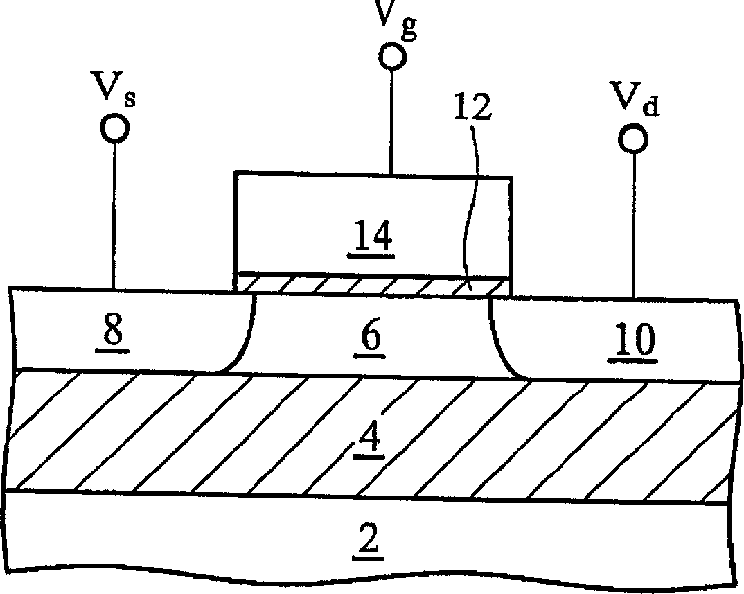
[0031] In order to make the above-mentioned purposes, features and advantages of the present invention more obvious and understandable, a preferred embodiment is specifically cited below, and in conjunction with the accompanying drawings, the detailed description is as follows:

[0032] The structure with Schottky source / drain according to the embodiment of the present invention and its manufacturing method are described below. The intermediate steps of the manufacturing method are illustrated schematically. Then explore the various variations and how they work. The numbers of all illustrations are in one-to-one correspondence with the objects described.

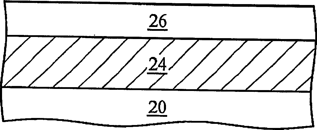
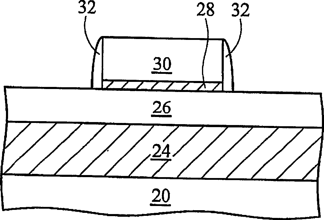
[0033] Figure 2 to Figure 5 are intermediate steps showing the manufacturing method according to the embodiment of the present invention. figure 2 A silicon-on-insulator structure is shown. An insulating layer (insulator) 24 is formed on a substrate (substrate) 20 . A semiconductor layer (semiconductor) 26 is formed o...


PUM


Abstract

A tunneling injection based Schottky source / drain memory cell comprising: a first semiconductor layer with a first conductivity type overlying an insulating layer, wherein the first semiconductor acts as a body region; a gate dielectric overlying the semiconductor layer; a gate electrode overlying the gate dielectric; a pair of spacers on sides of the gate electrodes; and a first Schottky barrier junction formed on a source region and a second Schottky barrier junction formed on a drain region on opposing sides of the body region. The source and the regions have an overlapping portion with the gate electrode and length of overlapping portion is preferably greater than about 5 AA. Interfacial layers are formed between the first and the second Schottky barrier regions.

Description

technical field [0001] The present invention relates to a dynamic random access memory, in particular to a dynamic random access memory unit with a single transistor without capacitance of Schottky source and drain. Background technique [0002] When embedded dynamic random access memory (DRAM) is applied to a system-on-chip (System-On-Chip), it has many advantages in terms of function, size and bandwidth. However, if a general DRAM cell, such as a DRAM cell composed of a single transistor and a stack or deep trench capacitor, is integrated into a standard logic complementary metal-oxide-semiconductor (CMOS) ) process, typically requires 5 to 8 additional masking steps, resulting in an additional cost of 25%. Fortunately, the recently developed capacitor-less single-transistor DRAM cells are used in embedded or non-embedded (stand-alone) architectures, because of their small size and fully suitable for CMOS process, relatively has many advantages. [0003] The capacitive ...

Claims


Application Information

Patent Timeline
Patent Type & Authority Applications(China)
IPC IPC(8): H01L27/108H01L29/78H01L29/40H01L21/8242H01L21/336
CPCH01L29/7841H01L27/095H01L27/108H01L27/10802H01L27/10844H01L29/812H10B12/20H10B12/01H10B12/00
Inventor 柯志欣陈宏玮李文钦季明华葛崇祜
Owner TAIWAN SEMICON MFG CO LTD
Why Eureka
Try Eureka