Eureka AIR delivers breakthrough ideas for toughest innovation challenges, trusted by R&D personnel around the world.

Illumination device

A lighting device and lighting field technology, applied in the field of marking devices, can solve the problems of expensive lighting devices, and achieve the effect of reducing installation

Active Publication Date: 2006-08-16
SIEMENS ELECTRONICS ASSEMBLY SYST LLC
View PDF1 Cites 4 Cited by
  • Summary
  • Abstract
  • Description
  • Claims
  • Application Information

AI Technical Summary

Problems solved by technology

The disadvantage of such an optical sensor device is that the lighting device comprising three lighting units can only be produced in a costly manner, since the corresponding luminous elements have to be mounted at different positions on different lighting planes within the lighting device

Method used


Image

  • Illumination device
  • Illumination device

Examples


Embodiment Construction

[0027] It should be noted here that, in the figures, the numbering of corresponding components differs only in the first digit.

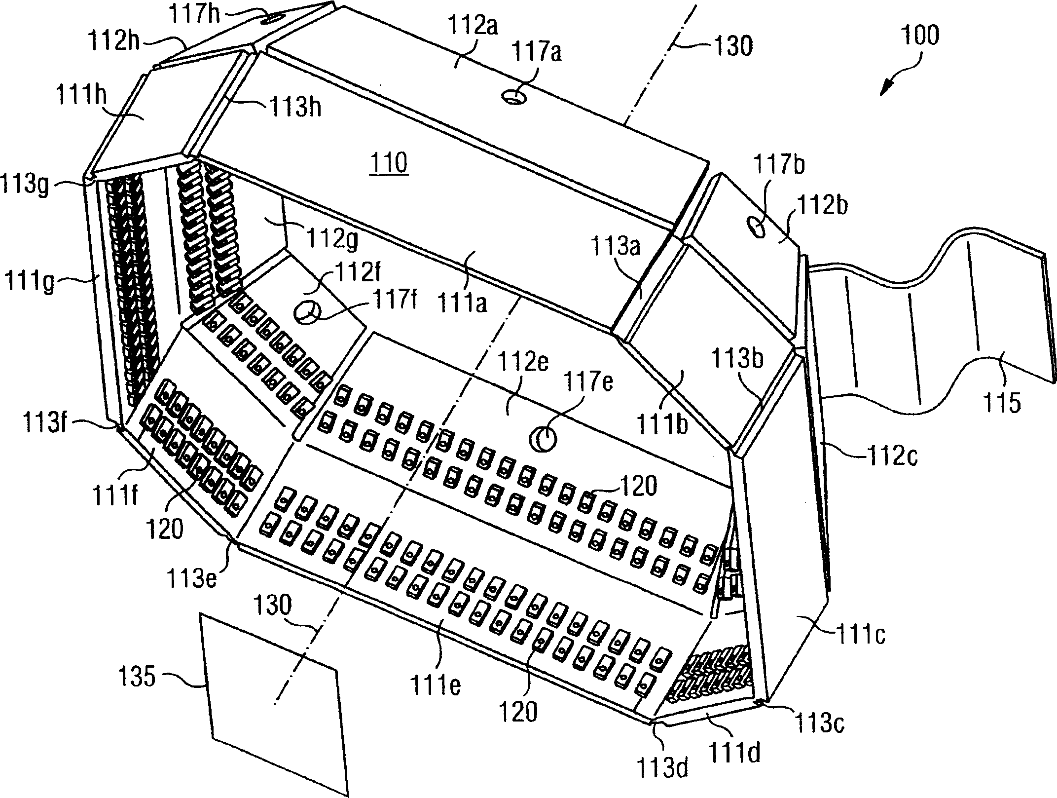
[0028] figure 1 A lighting device 100 is shown, which has a circuit carrier 110 on which a plurality of different light emitting diodes 120 are mounted. The circuit carrier 110 is octagonal, and the rigid regions 111a, 111b, 111c, 111d, 111e, 111f, 111g, 111h are connected by seven flexible intermediate regions 113a, 113b, 113c, 113d, 113e, 113f, 113g . Every two adjacent rigid regions 111 form an angle with each other, and the right side of the rigid region 111h is at least almost touching the left side of the rigid region 111a. In this way, the rigid region 111 a of the circuit carrier 110 forms an almost closed octagon symmetrical about the optical axis 130 . On the optical axis 130 there is an illumination field 135 , which is illuminated by the illumination device 100 with a sufficiently uniform light intensity from different illumination an...


PUM


Abstract

The invention relates to an illumination device, in particular to an illumination electronic component and / or a marked illumination device loaded on a component, which comprises a first illumination unit (111e) and a second illumination unit (111f), wherein the first illumination unit includes at least one first illumination element (120) arranged on a first illumination plane, and the second illumination element includes at least one second illumination element arranged on a second illumination plane. The illumination elements are arranged on a common circuit carrier (110), the common circuit carrier includes at least one planar first rigid region (111e) and a planar second rigid region (111f), and the two rigid regions are connected with each other at a certain angle through a flexible intermediate region (113e) on the common circuit carrier (110). The first rigid region is the first illumination unit, and the second rigid region is the second illumination unit thus illuminating an illumination field (135) from different illumination directions. The invention can be used for achieving the illumination device suitable for various illumination conditions and achieve compact structure form by simple installation.

Description

technical field [0001] The invention relates to a device for illuminating objects, in particular electronic components and / or markings mounted on component carriers, from different directions. Background technique [0002] When placing components automatically in so-called automatic component placement machines, the component conveyor supplies components to predetermined pick-up positions. There, the placement or insertion head picks up the components, which can be freely positioned in the working area with the aid of a positioning system. The placement head sends the picked components to the assembly position and places them on the loading position determined by the corresponding connection surface of the component carrier to be assembled. [0003] As electronic components become smaller and smaller, accurate optical position measurement of the components picked up by the placement head is required in the precise component placement process, so that the placement head can ...

Claims


Application Information

Patent Timeline
Patent Type & Authority Applications(China)
IPC IPC(8): H05K13/08
CPCG01N2021/8845H05K2201/046H05K2201/10106G01N21/8806H05K1/189G01N2201/062
Inventor K·-H·贝施D·雷克滕瓦尔德C·肖尔
Owner SIEMENS ELECTRONICS ASSEMBLY SYST LLC
Why Eureka
Eureka Blog
Learn More