Micronano transfer device

A micro-nano, mold technology, applied in the direction of optics, opto-mechanical equipment, instruments, etc., can solve the problems that affect the forming quality of forming materials, the complexity of light source design mechanism, and the small transfer area, so as to improve the industrial utilization value and design more Effects of flexibility and equipment cost reduction

Inactive Publication Date: 2006-09-13
IND TECH RES INST
View PDF2 Cites 1 Cited by
  • Summary
  • Abstract
  • Description
  • Claims
  • Application Information

AI Technical Summary

Problems solved by technology

In this way, not only the processing cost before and after transfer is increased, but also the process control is incoherent, and the forming cycle is prolonged, which is not conducive to mass production
[0011] In addition, the light transmittance of the sealing sleeve is usually poor, so when the ultraviolet light must pass through the light-permeable window and then pass through the sealing sleeve, the energy of the ultraviolet light will be absorbed or even scattered during the transmission process.
Like this, because this prior art can't control the ultraviolet light energy that provides, and can't obtain uniform transfer printing finished product, affect the forming quality of forming material
[0012] Therefore, due to the disadvantages of the above-mentioned prior art, such as complex light source design mechanism, expensive equipment cost, small transfer area, increased processing cost, incoherent process control, prolonged molding cycle, and difficult control of molding quality, resulting in high cost, low productivity, and poor quality Not good and not conducive to mass production, so there are urgent improvements

Method used


Image

  • Micronano transfer device
  • Micronano transfer device
  • Micronano transfer device

Examples


Embodiment 1

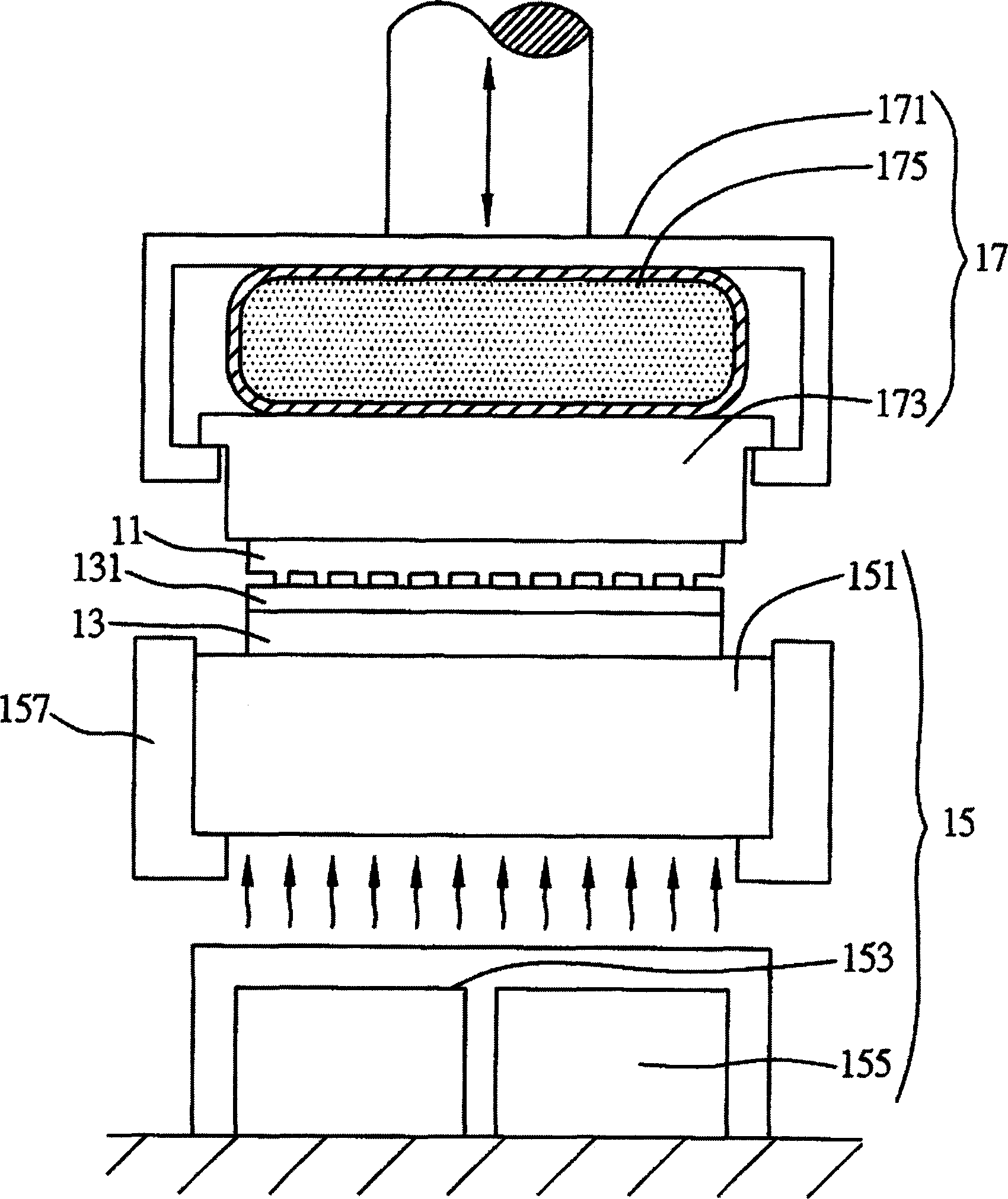
[0033] figure 1It is drawn according to Embodiment 1 of the micro-nano transfer device of the present invention. It should be noted that the micro-nano transfer printing device of the present invention is used to transfer nano-scale structures. The following examples use a micro-nano transfer printing device that can manufacture nanostructures with a characteristic structure size below 100 microns as an example for illustration, but Not limited to this. Since the existing nanostructures are all applicable objects, their structures have not changed, so for the sake of simplification, the features and structures of the present invention are clearer and easier to understand. In the accompanying drawings, only the structures directly related to the present invention are shown, and the rest Omit.

[0034] Such as figure 1 As shown, the micro / nano transfer device of this embodiment at least includes: a mold 11 , a substrate 13 and an energy transfer module 15 .

[0035] The di...

Embodiment 2

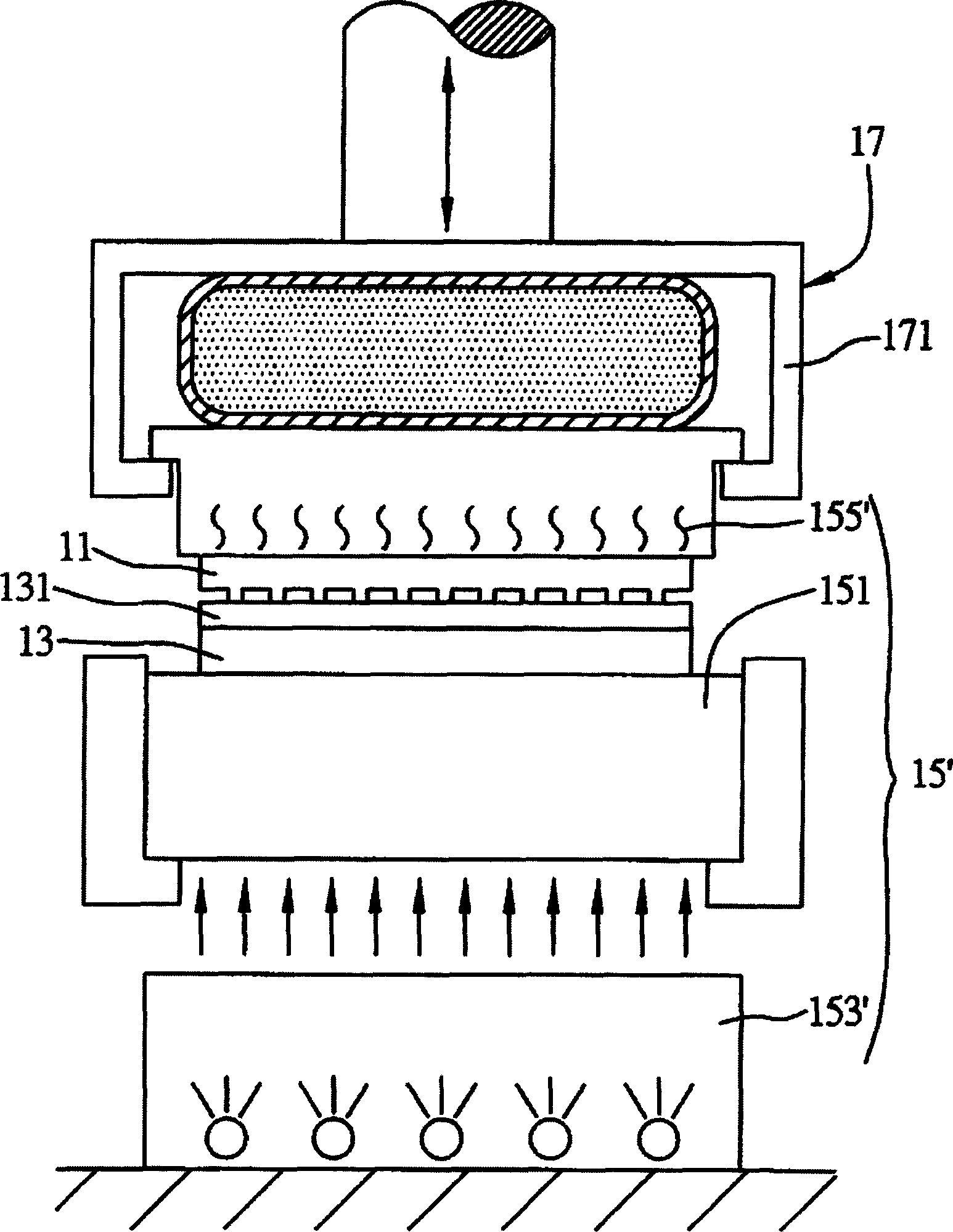
[0047] figure 2 It is drawn according to Embodiment 2 of the micro-nano transfer device of the present invention. Wherein, the same or similar components as in Embodiment 1 are represented by the same or similar component symbols.

[0048] The biggest difference between Embodiment 2 and Embodiment 1 is that Embodiment 1 uses an energy transfer module with two energy sources on the same side, while Embodiment 2 can form an energy transfer module with two energy sources on different sides.

[0049] Such as figure 2 As shown, the micro / nano transfer device of this embodiment at least includes: a mold 11, a substrate 13, and an energy transfer module 15'. The energy transfer module 15' includes the energy transfer member 151, an energy source 153', and an energy source 155'. The energy source 153' can be, for example, an ultraviolet light source, and the energy source 155' can be a heating element that can hold the mold 11. source, and the energy source 155' can be set on the...

Embodiment 3

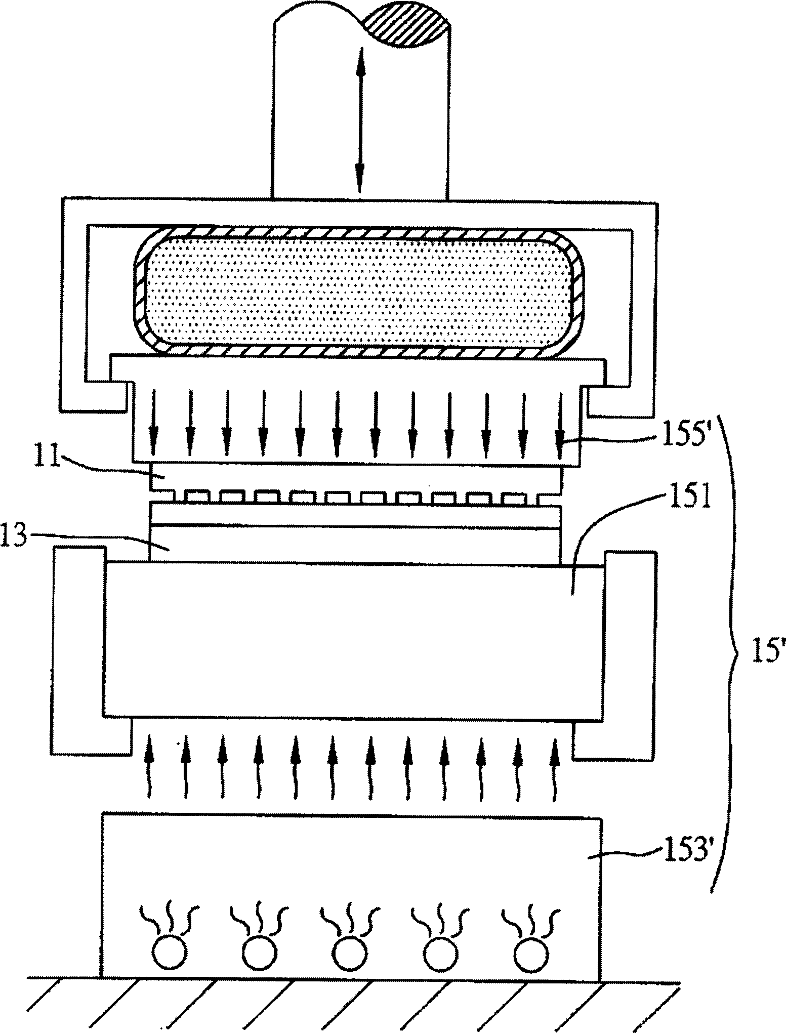
[0052] image 3 It is drawn according to Embodiment 3 of the micro-nano transfer device of the present invention. Wherein, the same or similar components as those in the above-mentioned embodiments are represented by the same or similar component symbols.

[0053] The biggest difference between embodiment 3 and embodiment 2 is that in embodiment 2, the energy source 153 ′ such as an ultraviolet light source is arranged below the energy transfer member 151 , and the energy source 155 ′ such as a heating source is arranged above the mold 11 In the third embodiment, the positions of the energy source 153' and the energy source 155' in the second embodiment are exchanged.

[0054] Such as image 3 As shown, in this embodiment, the energy transfer module 15 ′, such as the energy source 155 ′ of the heating source, is arranged below the energy transfer member 151 , and the energy source 153 ′, such as an ultraviolet light source, is arranged above the mold 11 . At this time, a mo...


PUM

PropertyMeasurementUnit
wavelengthaaaaaaaaaa

Abstract

A micro-nano reprinting device consists of mould, base plate with a forming material layer and energy transfer module with energy transfer piece as well as an energy source. It is featured as connecting energy transfer piece to base plate for providing reprint energy to base plate by energy source to let partial reprint energy penetrate energy transfer piece up to base plate for carrying out reprint - formation of said forming material layer.

Description

technical field [0001] The invention relates to a transfer printing device, in particular to a micro-nano transfer printing device. Background technique [0002] In the past ten years, the semiconductor industry has played a very important role in the global economy, and the development and application of various micro-electromechanical products have been driven by the development of semiconductor technology. However, as the line width and line spacing of various products are gradually reduced to less than 100 nanometers, the existing photolithography process (Photo-lithography) has encountered physical obstacles to optical imaging, the difficulty of process technology and the cost of production equipment And thus multiplied. At the same time, although the next-generation lithography technology (Next-generation lithography) has been proposed, this technology still has problems such as high equipment cost and low production capacity. Therefore, the currently widely concerne...

Claims


Application Information

Patent Timeline
Patent Type & Authority Applications(China)
IPC IPC(8): G03F7/00H01L21/027
Inventor 何侑伦陈来胜王维汉巫震华陈钏锋陈守仁
Owner IND TECH RES INST
Why Eureka
Try Eureka