

Double-sided wiring board fabrication method, double-sided wiring board, and base material therefor
一种印制电路板、制造方法的技术,应用在印刷电路制造、多层电路制造、印刷电路等方向,能够解决难以形成微细布线等问题
- Summary
- Abstract
- Description
- Claims
- Application Information
AI Technical Summary
Problems solved by technology
Method used
Image

Examples
Embodiment 1
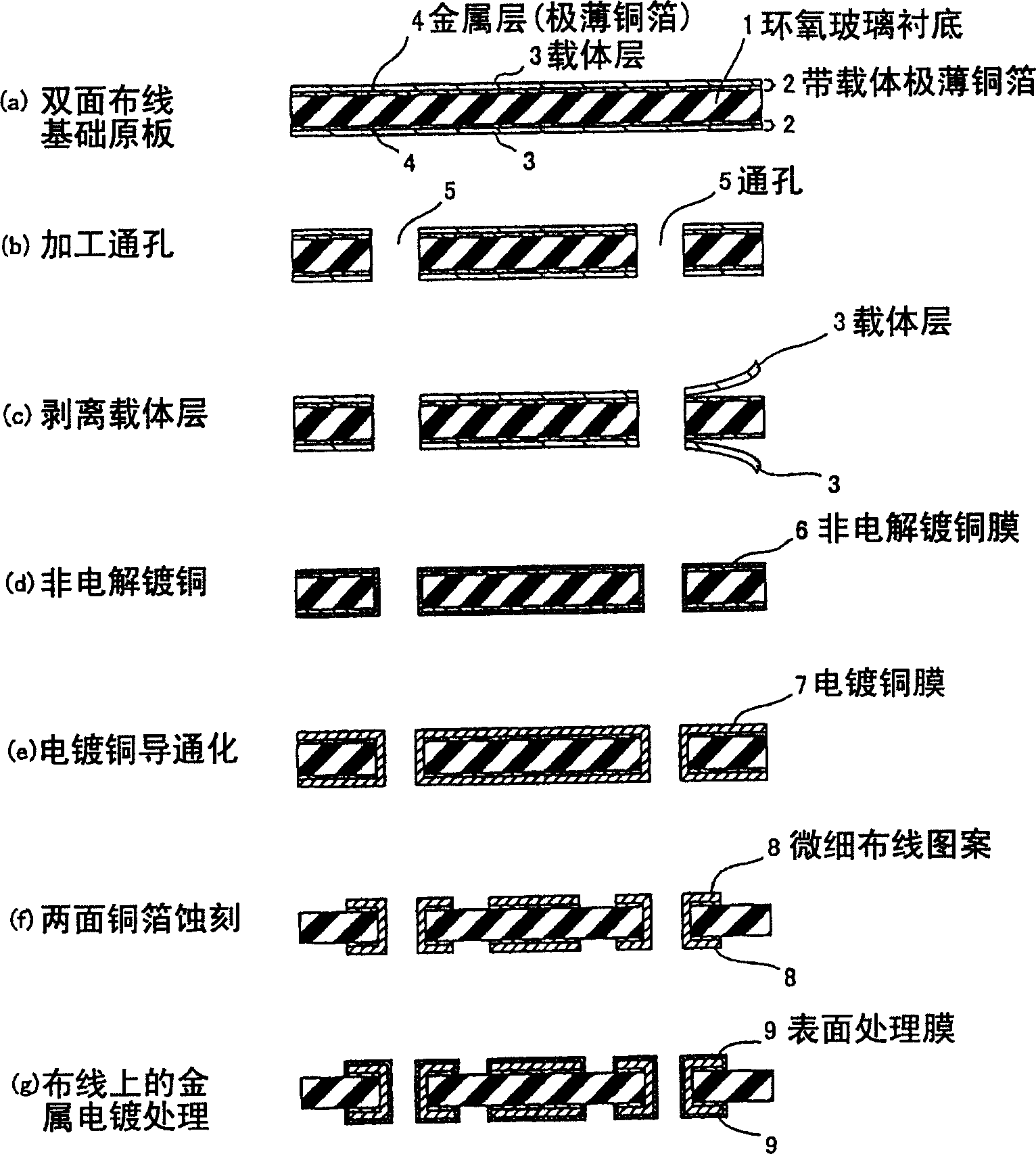
[0061] figure 1 (a)~ figure 1 (g) is a cross-sectional view of the manufacturing method (each process) of the double-sided wiring printed wiring board of Example 1 using a glass epoxy substrate (through-hole processing).
[0062] A glass epoxy substrate 1 having a thickness of 100 μm and a size of 500×500 mm was prepared. The epoxy resin is in a semi-hardened state (B-grade state).
[0063] An ultra-thin copper foil 2 with a carrier (trade name: "CopperBond Extra Thin Foil", manufactured by O-Rinbras Co., Ltd., Japan) was bonded to the upper and lower surfaces of the substrate 1 by hot pressing, so that it sandwiched the epoxy resin. Glass substrate1. The copper foil 2 is composed of an ultra-thin copper foil 4 (3 μm) / peelable layer / carrier copper foil 3 (18 μm). The bonding of the glass epoxy substrate 1 and the ultra-thin copper foil 2 with the carrier is by pasting the surface of the ultra-thin copper foil 4 on the glass epoxy substrate 1 ( figure 1 (a)) proceed.
...
Embodiment 2
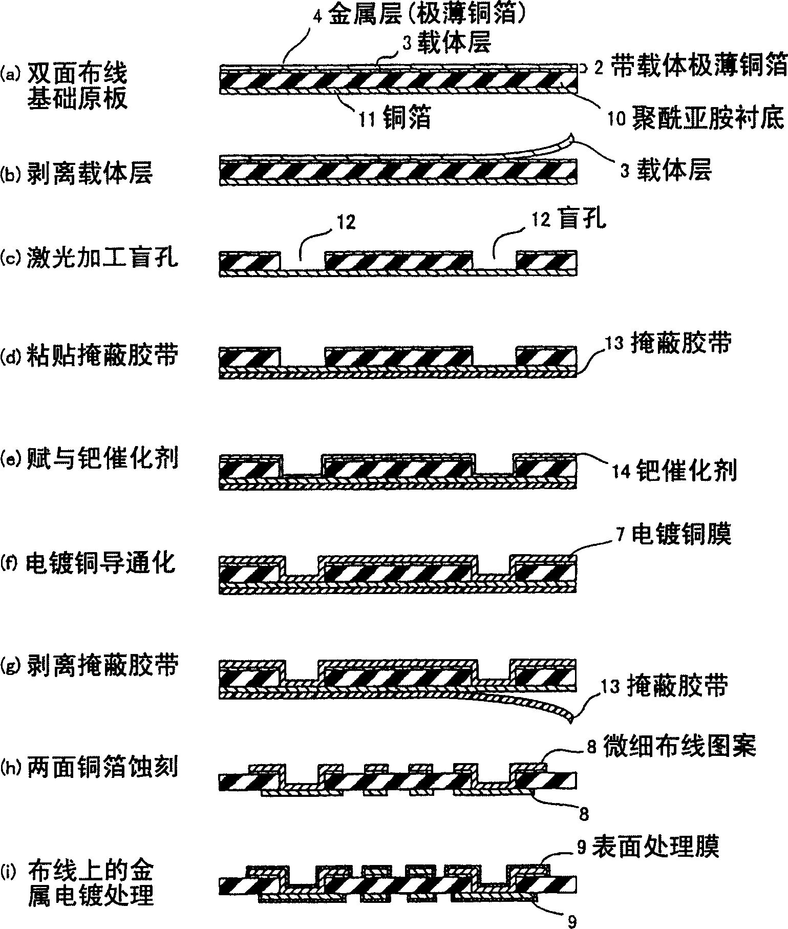
[0071] figure 2 (a)~ figure 2 (i) is a sectional view of the manufacturing method (each process) of the double-sided wiring printed wiring board (double-sided wiring flexible printed wiring board) of Example 2 using a polyimide substrate (blind via processing).
[0072] A thermoplastic polyimide-based adhesive was applied to both sides, and a polyimide tape (polyimide substrate 10 ) having a total thickness of 25 μm and a width of 70 mm was prepared for tens of meters.
[0073] An ultra-thin copper foil 2 with a carrier (trade name: "CopperBond Extra Thin Foil", manufactured by O-Linburas Co., Ltd., Japan) was bonded to one side of the substrate 10 by hot pressing, and an electrolytic copper foil with a thickness of 12 μm was bonded. 11 is pasted on the other side of the substrate 10, so that the two clamp the polyimide substrate 10 ( figure 2 (a)). The ultra-thin copper foil 2 with a carrier is composed of an ultra-thin copper foil 4 (3 μm) / peelable layer / carrier copper...
Embodiment 3
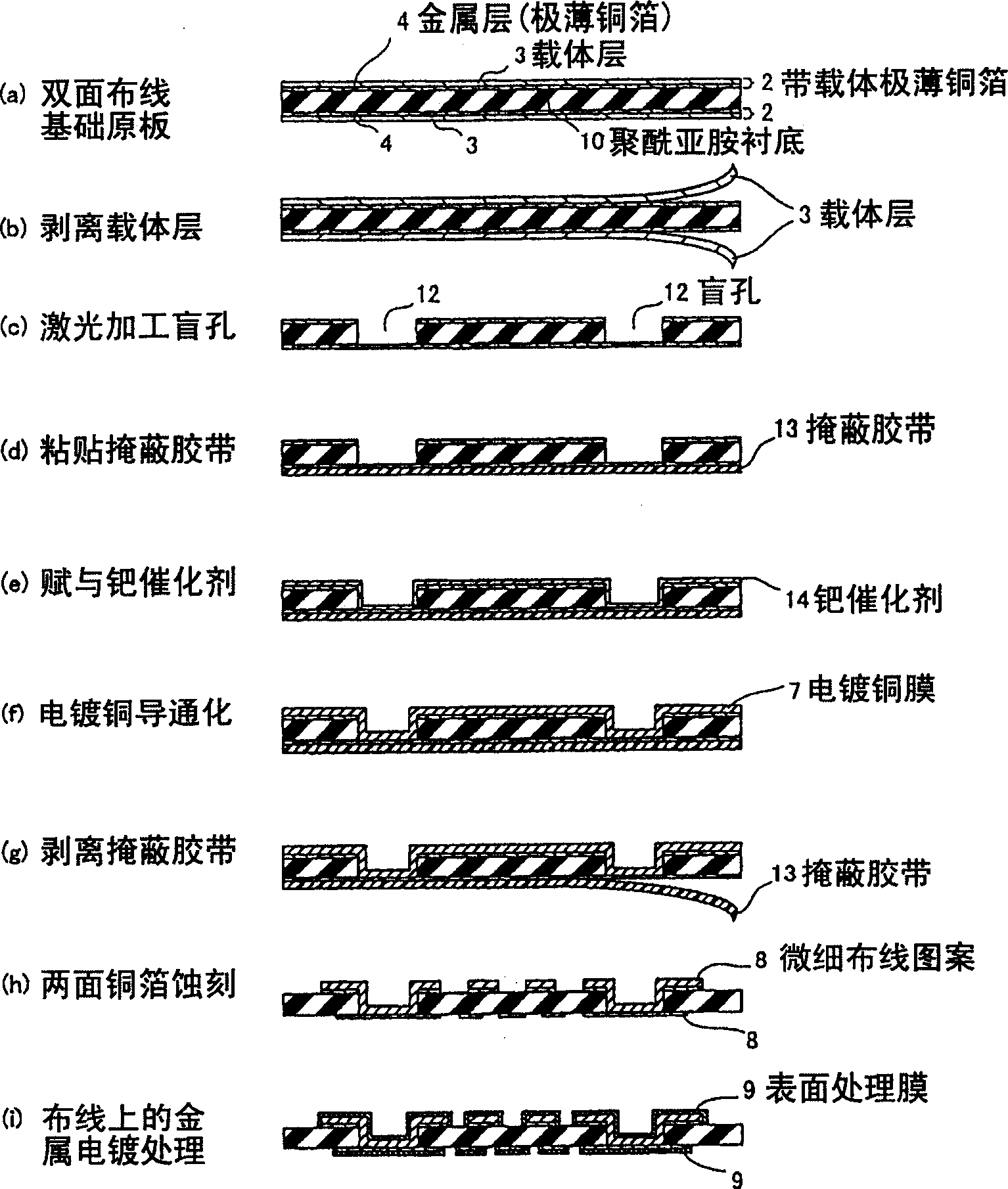
[0083] image 3 (a)~ image 3 (i) is a cross-sectional view of the manufacturing method (each process) of the double-sided wiring printed wiring board (double-sided wiring flexible printed wiring board) of Example 3 using a polyimide substrate (blind via processing) .
[0084] A thermoplastic polyimide adhesive was applied to both sides, and a polyimide tape (polyimide substrate 10 ) having a total thickness of 25 μm and a width of 70 mm was prepared for tens of meters.
[0085] An ultra-thin copper foil 2 with a carrier (trade name: "CopperBond Extra Thin Foil", manufactured by O-Linburas Co., Ltd., Japan) was bonded to both sides of the substrate 10 by hot pressing, so that the polyimide film was sandwiched between them. Substrate 10 ( image 3 (a)). The ultra-thin copper foil 2 with a carrier is composed of an ultra-thin copper foil 4 (3 μm) / peelable layer / carrier copper foil 3 (18 μm). The polyimide substrate 10 and the ultra-thin copper foil with carrier 2 are bonded...
PUM
 Abstract
Description
Claims
Application Information