Selective electroless-plated copper metallization

a technology of electroless plated copper and selective metallization, which is applied in the direction of semiconductor devices, semiconductor/solid-state device details, electrical apparatus, etc., can solve the problems of increasing the number of process steps involved in the fabrication of integrated circuits, affecting the quality of deposited materials, and reducing the amount of deposited conductive materials. , to achieve the effect of reducing the amount of deposited conductive materials and alleviating important environmental concerns

Inactive Publication Date: 2005-02-03
MICRON TECH INC
View PDF99 Cites 47 Cited by
  • Summary
  • Abstract
  • Description
  • Claims
  • Application Information

AI Technical Summary

Benefits of technology

[0009] The above mentioned problems associated with integrated circuit size and performance, the via and metal line formation process, and other problems are addressed by the present invention and will be understood by reading and studying the following specification. Structures and methods are provided which include a selective electroless copper metallization. The present invention provides for a multilayer copper wiring structure by electroless, selectively deposited copper in a streamlined process which will not require chemical mechanical planarization (CMP). Thus, the present invention significantly reduces the amount of deposited conductive material, e.g. copper, which is ultimately discarded according to conventional processes. This alleviates important environmental concerns regarding the disposition of used materials. Further, by avoiding the need for a CMP process step, the usage of consumables such as pads and slurry is conserved.

Problems solved by technology

During the CMP process, especially for the via holes, more than 99% of the deposited copper is removed, and this is a very wasteful and expensive process, which includes a high usage of consumables such as pads and slurry.
Furthermore, the disposition of used materials is a very important environmental issue.
All of these above described methods are rather complex which means that the number of process steps involved in integrated circuit fabrication increases.
The problem associated with these methods is that an increase in the number of process steps makes integrated circuit fabrication more costly.
Further, none of the above described methods address or provide a resolution to the costly excess expenditure of materials and the environmental concerns when such processes are implemented to form sub-micron vias and metal lines on wafers in a conventional CMP fabrication process.

Method used


Image

  • Selective electroless-plated copper metallization
  • Selective electroless-plated copper metallization
  • Selective electroless-plated copper metallization

Examples


Embodiment Construction

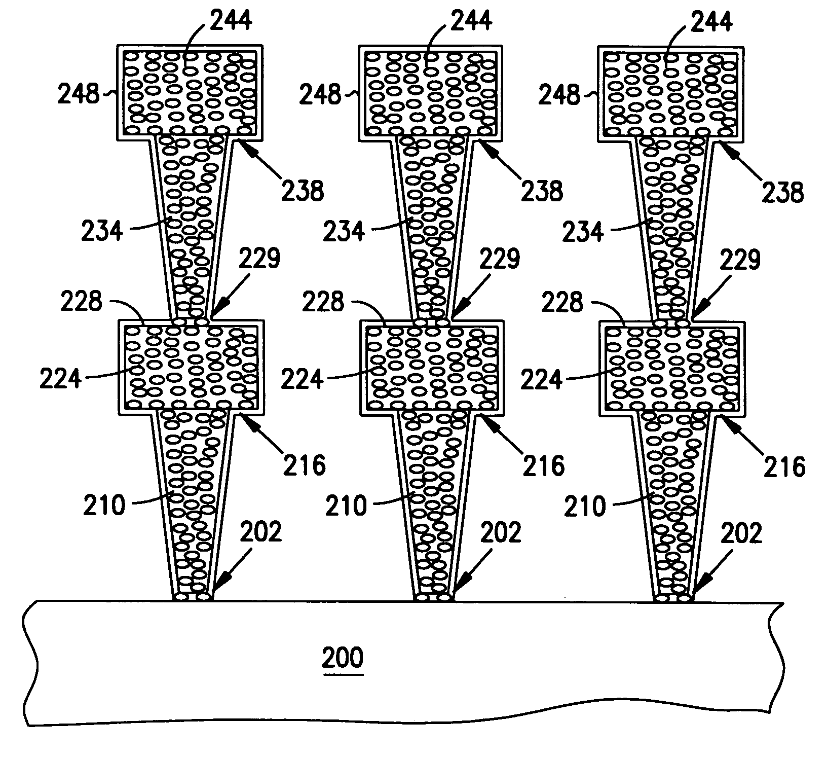
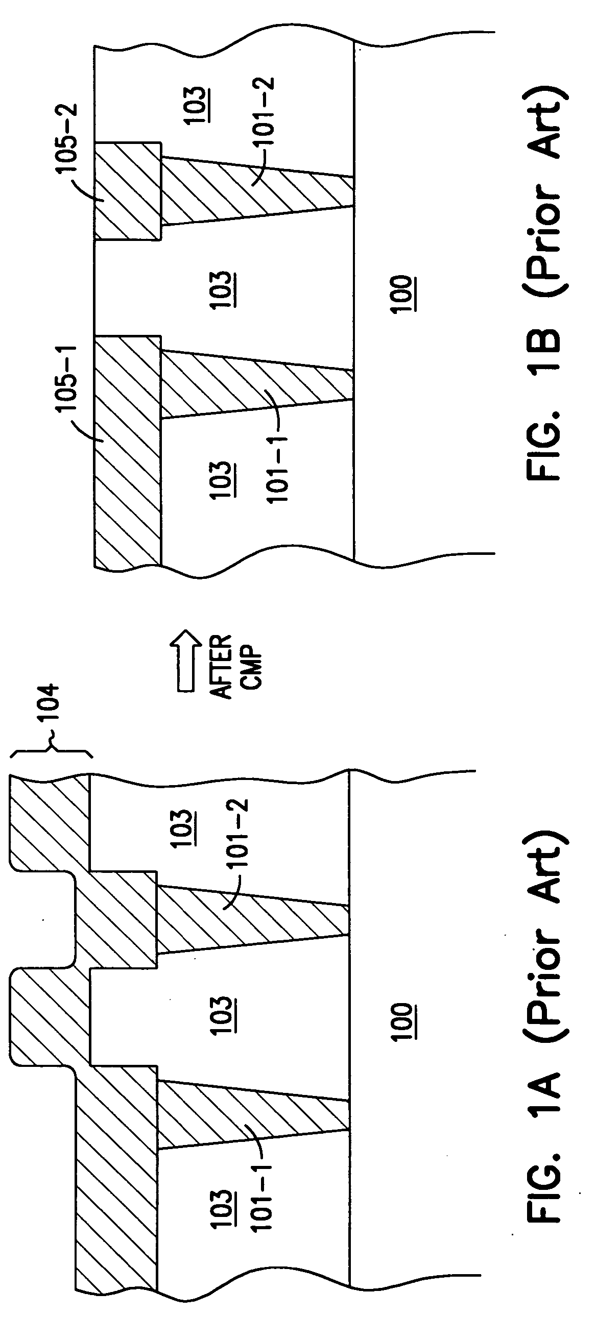
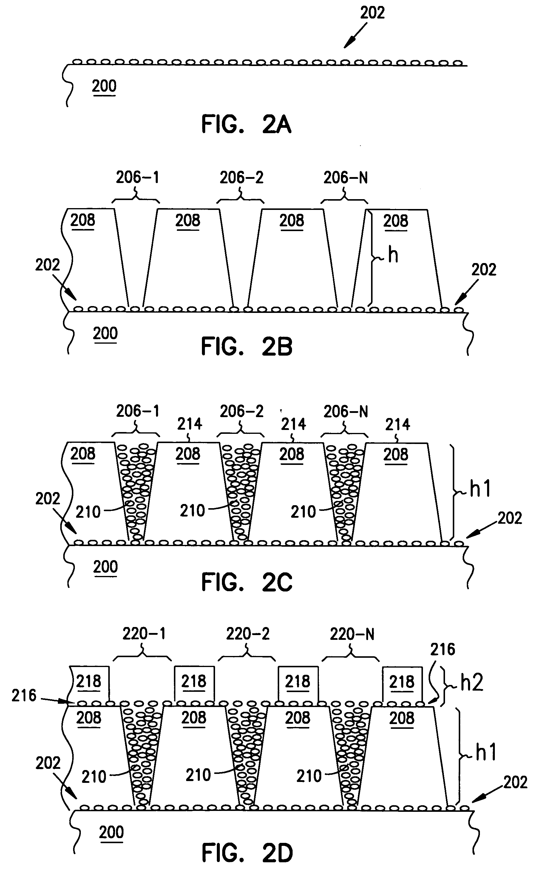
[0016] In the following detailed description of the invention, reference is made to the accompanying drawings which form a part hereof, and in which is shown, by way of illustration, specific embodiments in which the invention may be practiced. These embodiments are described in sufficient detail to enable those skilled in the art to practice the invention. Other embodiments may be utilized and structural, logical, and electrical changes may be made without departing from the scope of the present invention.

[0017] The terms wafer and substrate used in the following description include any structure having an exposed surface with which to form the integrated circuit (IC) structure of the invention. The term substrate is understood to include semiconductor wafers. The term substrate is also used to refer to semiconductor structures during processing, and may include other layers that have been fabricated thereupon. Substrate include doped and undoped semiconductors, epitaxial semicond...


PUM

PropertyMeasurementUnit
thicknessaaaaaaaaaa
thicknessaaaaaaaaaa
thicknessaaaaaaaaaa

Abstract

Structures and methods are provided which include a selective electroless copper metallization. The present invention includes a novel methodology for forming copper vias on a substrate, including depositing a thin film seed layer of Palladium (Pd) or Copper (Cu) on a substrate to a thickness of less than 15 nanometers (nm). A number of via holes is defined above the seed layer. A layer of copper is deposited over the seed layer using electroless plating to fill the via holes to a top surface of the patterned photoresist layer. The method can be repeated any number of times, forming second, third and fourth layers of copper. The photoresist layers along with the seed layers in other regions can then be removed, such as by oxygen plasma etching, such that a chemical mechanical planarization process is avoided.

Description

RELATED APPLICATIONS [0001] This application is a Divisional of U.S. application Ser. No. 09 / 483,881, filed Jan. 18, 2000, which is incorporated herein by reference. [0002] This application is related to the following co-filed and commonly assigned applications; U.S. application Ser. No. 09 / 488,098, filed Jan. 18, 2000, now U.S. Pat. No. 6,429,120 and U.S. application Ser. No. 09 / 484,303, filed Jan. 18, 2000, both of which are hereby incorporated by reference.FIELD OF THE INVENTION [0003] The present invention relates generally to integrated circuits. More particularly, it pertains to structures and methods for selective electroless-plated copper metallization. BACKGROUND OF THE INVENTION [0004] The rapid progress in miniaturization of integrated circuits (IC) is leading to denser and finer pitched chips with ever increasing performance. In order to enhance the performance of advanced ICs, the interconnect systems are gradually migrating from aluminum-based metallurgy to higher-cond...

Claims


Application Information

Patent Timeline
Patent Type & Authority Applications(United States)
IPC IPC(8): H01L23/532
CPCH01L21/288H01L21/7682H01L21/76852H01L21/76874H01L21/76879H01L23/4821H01L2924/0002H01L23/5222H01L23/53238H01L2924/00H01L21/76885
Inventor AHN, KIE Y.FORBES, LEONARD
Owner MICRON TECH INC
Why Eureka
Try Eureka