Process for electrodeposition of copper chip to chip, chip to wafer and wafer to wafer interconnects in through-silicon vias (TSV)

A technology of electrodeposition and process, which is applied in the field of high-purity copper electrolysis to form a conductor structure in through-silicon vias, which can solve problems such as wafer bending or deformation, uneven deposition, deformation, etc., to minimize stress and avoid dopants and the effect of stomata

Inactive Publication Date: 2012-01-11
ATOTECH DEUT GMBH
View PDF2 Cites 50 Cited by
  • Summary
  • Abstract
  • Description
  • Claims
  • Application Information

AI Technical Summary

Problems solved by technology

Attempts to electrodeposit high-purity copper into such high-aspect-ratio TSVs have been partially successful, but have been plagued by problems caused by (a) internal stresses in the copper deposition that can cause wafer bowing or deformation, (b) non-uniform deposition (i.e., grain boundaries, crystal structure defects, etc.), (c) gas (porosity) in the body of electrodeposited copper and / or dopant of the plating bath liquid, and (d) Additional metal deposition at the entrance and exit of TSV perforations
[0004] Of these issues, the internal stress issue (a) may be the most problematic as it causes bowing and deformation throughout the silicon substrate where the TSVs are formed, and it can cause failure of the entire 3D arrangement
This failure may not occur until after the entire device has been fabricated, resulting in the loss not only of the failed silicon substrate, but of the entire device that had been incorporated into the silicon substrate at the time of failure

Method used


Image

  • Process for electrodeposition of copper chip to chip, chip to wafer and wafer to wafer interconnects in through-silicon vias (TSV)
  • Process for electrodeposition of copper chip to chip, chip to wafer and wafer to wafer interconnects in through-silicon vias (TSV)
  • Process for electrodeposition of copper chip to chip, chip to wafer and wafer to wafer interconnects in through-silicon vias (TSV)

Examples


example 1

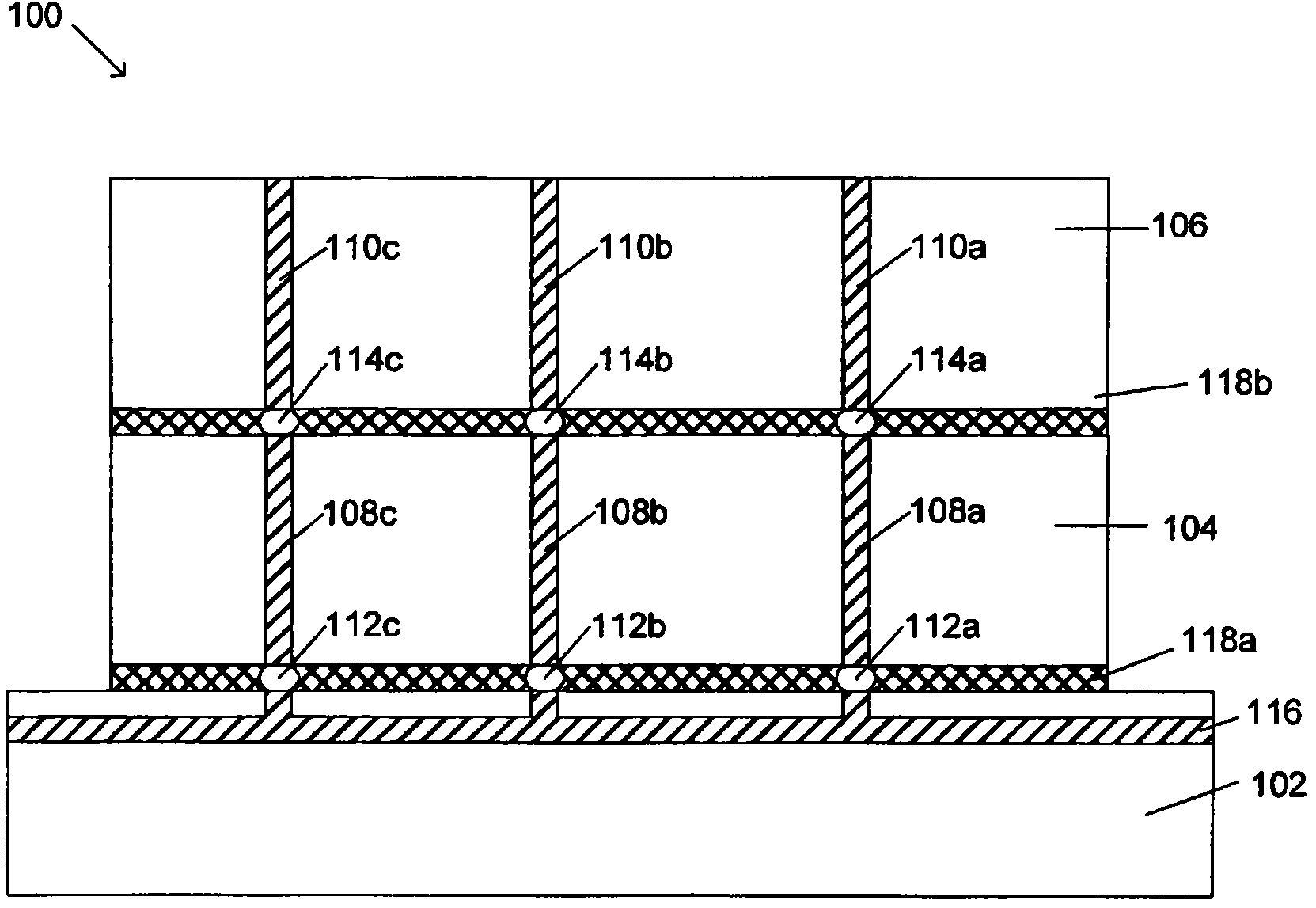
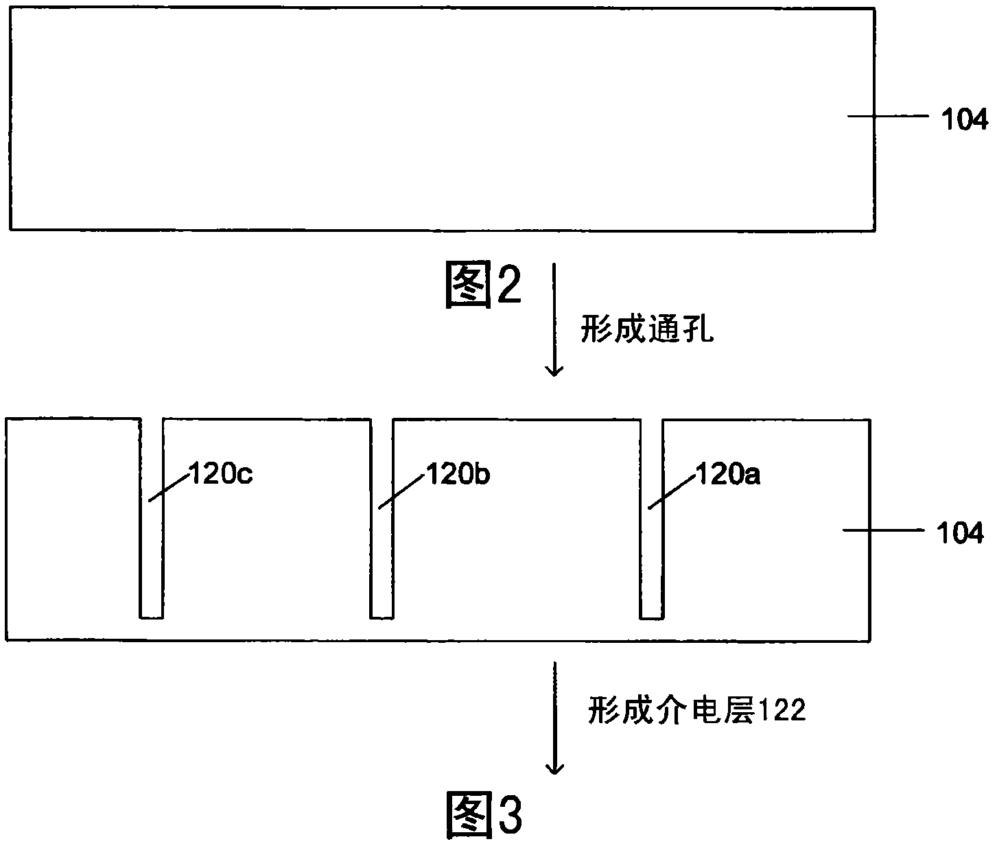
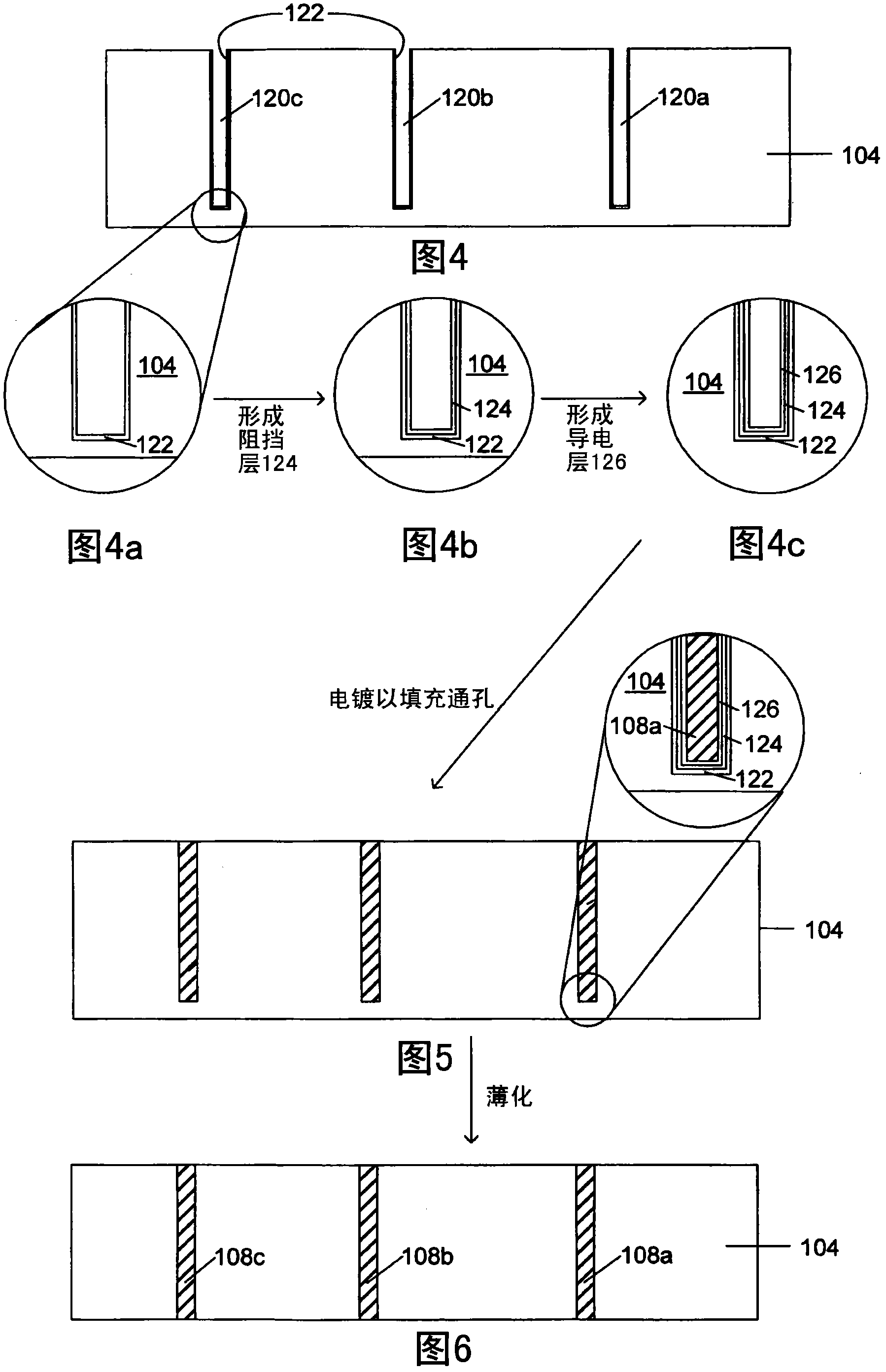
[0173]To create TSVs filled with high-purity copper deposits, the wafer is provided with vias with a diameter of approximately 10 microns and a depth of approximately 50 microns. The via is initially coated with a dielectric layer of silicon dioxide formed from high temperature oxidation of the inner sidewalls of the via. The dielectric layer on the inner sidewalls of the via is then coated with a diffusion barrier formed by sputtering from tantalum nitride. Subsequently, the diffusion barrier layer was coated with a copper base metal layer by a sputtering process, wherein the thickness of the copper base deposition layer was about 0.1 microns. The wafer was then dipped into the copper deposition bath described below in which the wafer was connected as a cathode and included an insoluble anode. The vias were filled with high purity copper by electrodeposition from a cell having the following composition to form TSVs according to the invention.

[0174] h 2 SO 4 , weight ra...

example 2

[0184] By using different electroplating methods of the cells disclosed above according to the present invention (these different electroplating methods or using similar cells but without the addition of Fe 2+ / Fe 3+ ions, or using a similar cell but with a soluble copper anode) where a pulsed current with the parameters shown in the table below was applied:

[0185]

[0186] The copper stress in the as-deposited TSV is:

[0187]

[0188] The internal stresses were measured after being deposited without a post annealing step. The measurements are the warpage and bow of the through-hole wafer (laser measurement). The facility used is a KLA-TENCOR FLX-2320 film stress measurement system, the thickness of the copper film is 1 micron, and the thickness of the wafer is 750 microns.

[0189] It is clearly shown by the data of Example 2 that when the TSVs are filled according to the invention, a significantly reduced and more significantly consistent stress level is obtained...


PUM

PropertyMeasurementUnit
thicknessaaaaaaaaaa
thicknessaaaaaaaaaa
thicknessaaaaaaaaaa

Abstract

A process of electrodepositing high purity copper in a via in a silicon substrate to form a through-silicon-via (TSV), including immersing the silicon substrate into an electrolytic bath in an electrolytic copper plating system in which the electrolytic bath includes an acid, a source of copper ions, a source of ferrous and / or ferric ions, and at least one additive for controlling physical-mechanical properties of deposited copper; and applying an electrical voltage for a time sufficient to electrodeposit high purity copper to form a TSV, in which a Fe+2 / Fe+3 redox system is established in the bath to provide additional copper ions to be electrodeposited by dissolving copper ions from a source of copper metal.

Description

technical field [0001] The present invention relates to a process for electrolytically forming a conductor structure from high-purity copper, in particular to electrolytically forming conductors in through-silicon vias (TSV) from high-purity copper when manufacturing devices such as MEMS or semiconductor devices structure. Such TSVs are useful, for example, in integrated circuits in stacked or 3D arrangements, where the TSVs provide electrical connections between layers of the device, where the TSVs have relatively large diameters, relatively large depths, and high aspect ratio. Background technique [0002] There is a continuing need to manufacture cheaper, smaller and lighter electronic products that offer better performance and improved functionality. The number of electronic devices on a single chip is still growing rapidly, and the ability of 2D layouts to accommodate these demands is being exceeded. According to the industrial roadmap, in 2010 the integrated circuit...

Claims


Application Information

Patent Timeline
Patent Type & Authority Applications(China)
IPC IPC(8): H01L21/288H01L21/768C25D3/38C25D5/18C25D7/12
CPCC25D21/16C25D5/02H01L21/76898C25D7/123C25D3/38C25D5/18H01L21/2885H01L2224/131H01L2224/16145H01L2224/16245H01L2224/05573H01L2224/13025H01L2224/05647H01L2924/00014H01L2224/0554H01L24/03H01L24/05C25D5/617C25D5/611H01L2924/014H01L2224/05599H01L2224/0555H01L2224/0556
Inventor 罗伯特·F·普赖塞尔
Owner ATOTECH DEUT GMBH
Why Eureka
Try Eureka