

Thimble device
A technology of thimble and ejector pin, which is applied in the manufacture of electrical components, semiconductor/solid state devices, circuits, etc. It can solve the problems of reduced work efficiency, chip damage and fragmentation, and the failure of the manipulator to transfer chips normally, so as to avoid chip jumping and production. inefficient effect
- Summary
- Abstract
- Description
- Claims
- Application Information
AI Technical Summary
Problems solved by technology
Method used
Image

Examples
Embodiment Construction
[0019] The specific implementation of the thimble device of the present invention will be further described in detail below in conjunction with the accompanying drawings, but it is not used to limit the protection scope of the present invention.
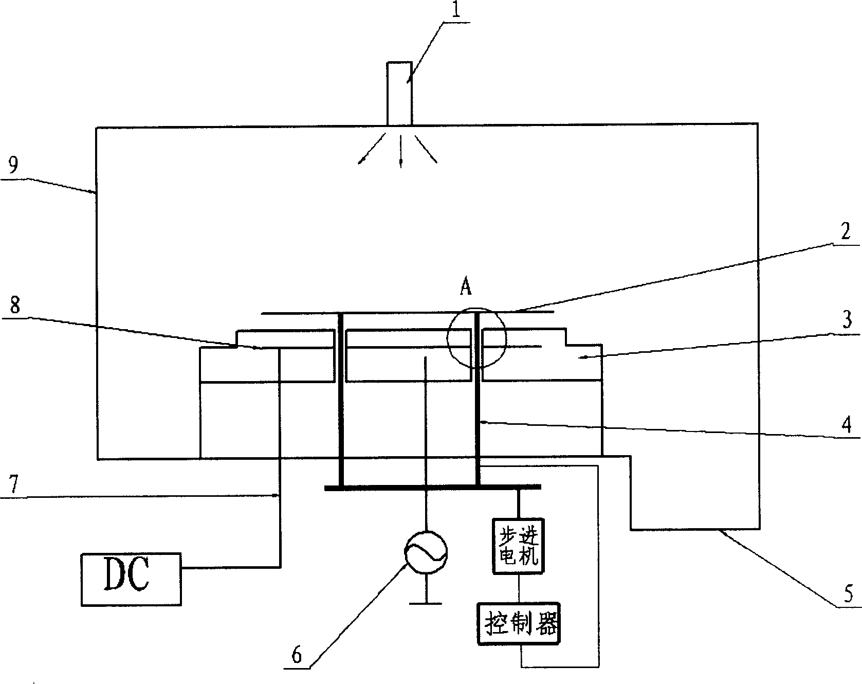
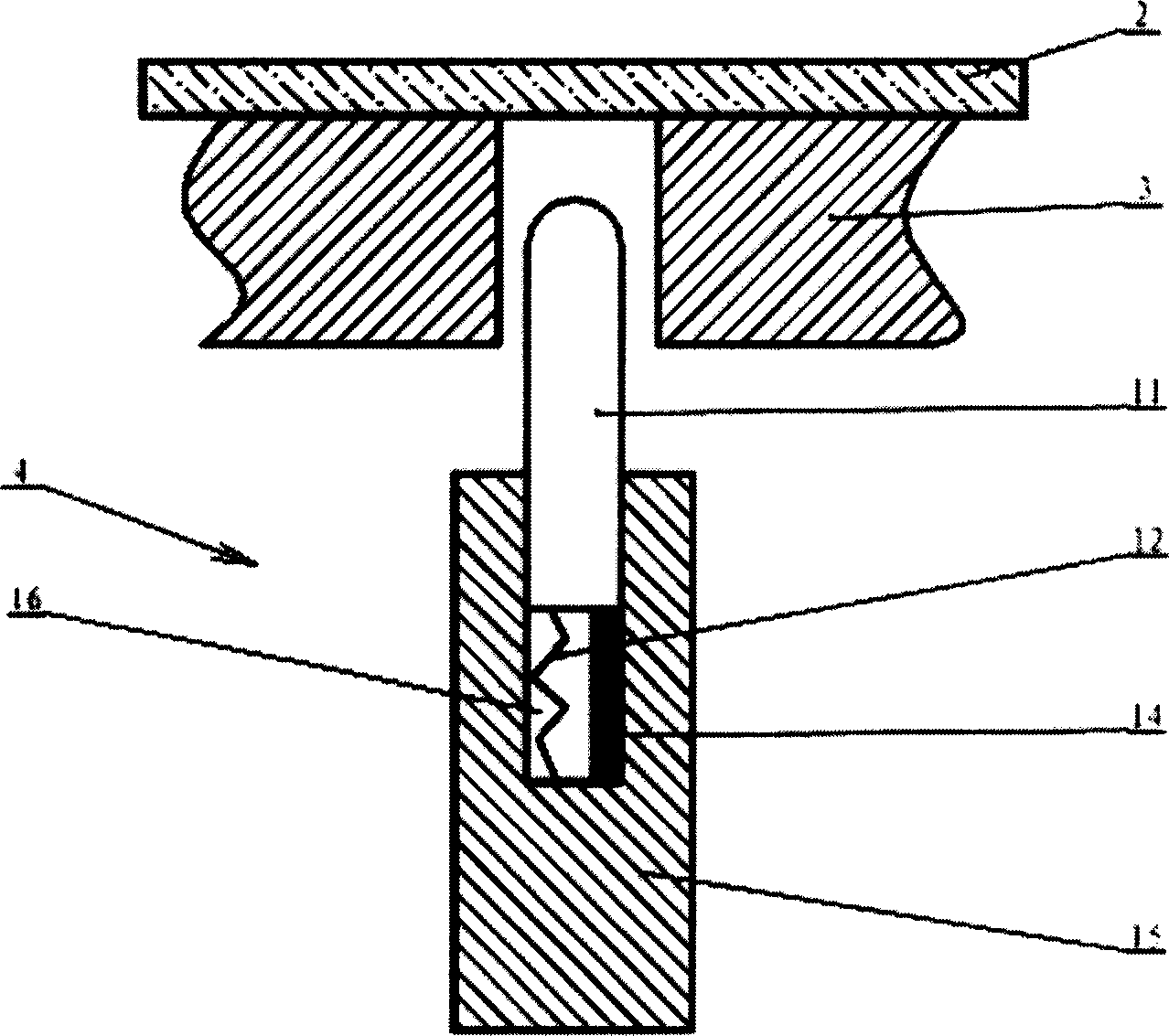
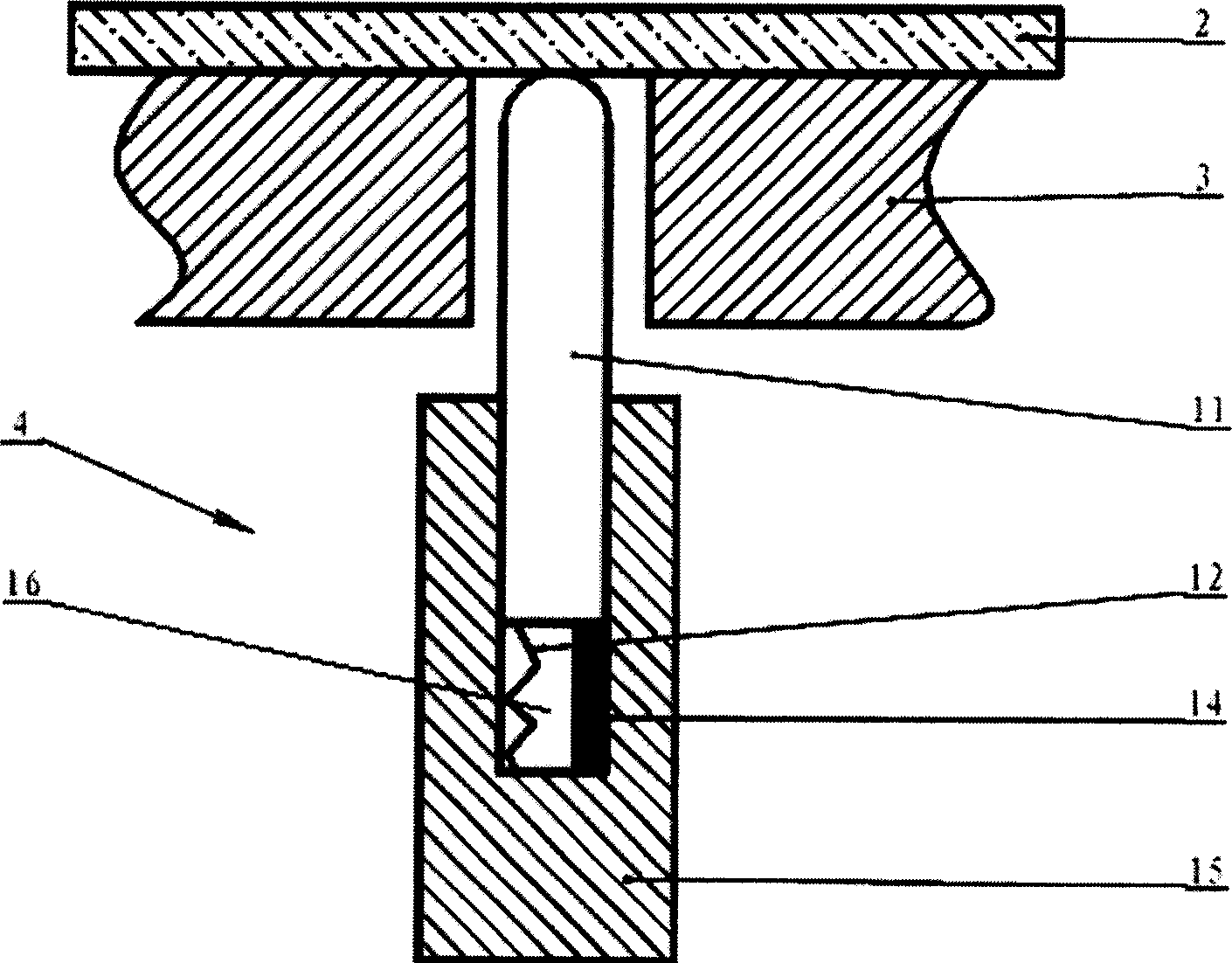
[0020] see figure 2 , image 3 and Figure 4 . The thimble device of the present invention includes a thimble 4, and the thimble 4 includes a thimble body 15 and a thimble rod 11, wherein a slot is provided in the thimble body 15, and the thimble rod 11 is inserted in the slot, and the thimble A space 16 is provided between the bottom end surface of the ejector rod 11 and the bottom wall of the slot. The height of the space 16 is 1 mm, and the height is feasible within the range of 0.5 mm to 2 mm. A spring 12 and a position sensor 14 are housed in the space 16 . The spring 12 can be replaced by other height deformers such as dampers. The force generated by the deformation of the spring 12 at about 0.1 mm is slightly greater tha...
PUM
 Abstract
Description
Claims
Application Information