Termoelectric crystal round plate

A chuck and wafer technology, applied in the direction of thermoelectric devices, circuits, electrical components, etc., can solve the problems of wafer thermal feedback and heating control ability, general products have no structure, no cooling function, etc.

Inactive Publication Date: 2006-11-01
TAIWAN SEMICON MFG CO LTD
View PDF0 Cites 5 Cited by
  • Summary
  • Abstract
  • Description
  • Claims
  • Application Information

AI Technical Summary

Problems solved by technology

However, general wafer chucks still have some disadvantages, such as weak thermal feedback and heating control capabilities of the wafer; little or no cooling function; and poor temperature control accuracy of the wafer
[0004] It can be seen that the above-mentioned existing thermoelectric wafer chuck obviously still has inconvenience and defects in structure and use, and needs to be further improved urgently.
In order to solve the above-mentioned problems, the relevant manufacturers have tried their best to find a solution, but no suitable design has been developed for a long time, and the general products do not have a suitable structure to solve the above-mentioned problems. This is obviously related. The problem that the industry is eager to solve

Method used


Image

  • Termoelectric crystal round plate
  • Termoelectric crystal round plate
  • Termoelectric crystal round plate

Examples


Embodiment Construction

[0051] In order to further explain the technical means and effects of the present invention to achieve the intended purpose of the invention, the specific implementation, structure, characteristics and features of the thermoelectric wafer chuck proposed according to the present invention will be described below in conjunction with the accompanying drawings and preferred embodiments. Efficacy, detailed as follows.

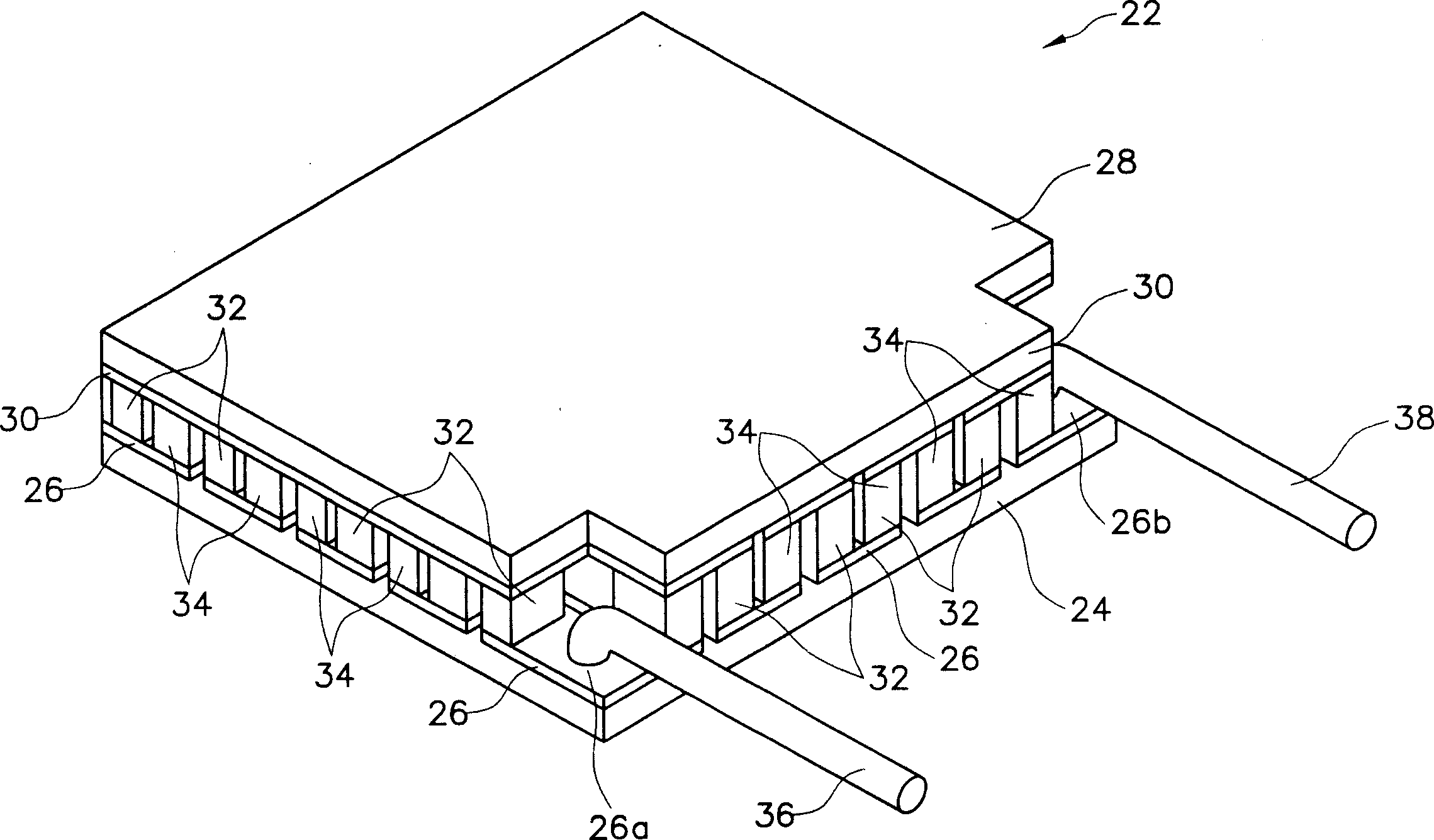
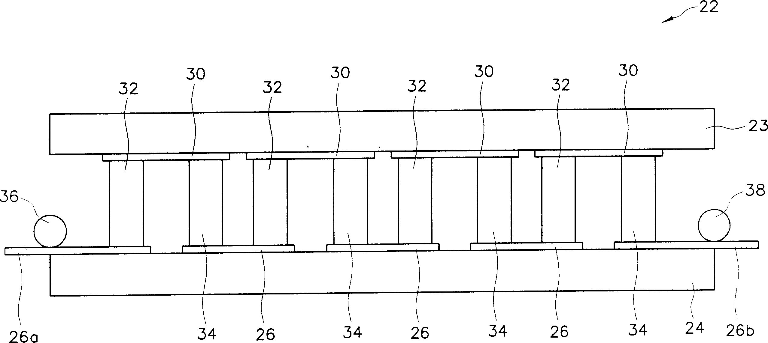
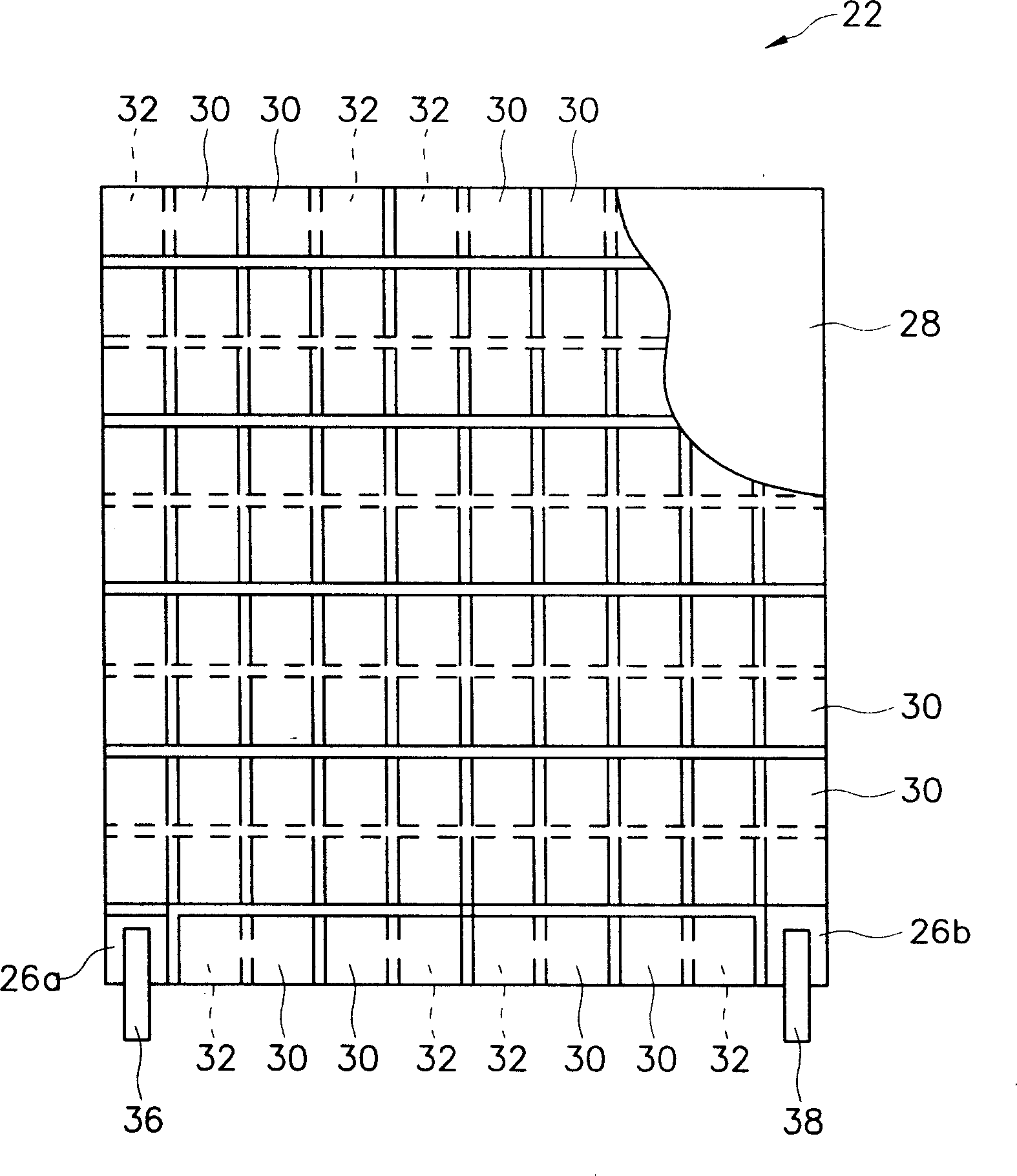
[0052] One aspect of the present invention is to provide a thermoelectric wafer chuck suitable for semiconductor manufacturing process. The thermoelectric wafer chuck has a chuck base and a wafer carrying surface. A plurality of fluid passages are conducted in the chuck base in a single-circuit or multi-circuit manner for distributing heating or cooling liquid. The thermoelectric module is in thermal contact with the wafer carrier surface. The thermoelectric module includes a plurality of P-type semiconductor connectors and a plurality of N-type semiconductor conn...


PUM


Abstract

A thermoelectric wafer chuck is disclosed. The thermoelectric wafer chuck includes a wafer support surface for supporting a wafer; and a thermoelectric module provided in thermal contact with the wafer support surface for heating and / or cooling the wafer support surface and wafer.

Description

technical field [0001] The present invention relates to a device for heating wafers in semiconductor manufacturing processes, in particular to a thermoelectric heating and cooling device for selectively heating or cooling wafers in semiconductor manufacturing processes, which has the advantage of fast and dynamic temperature Control capability, and at the same time have the ability to execute multi-zone temperature control. Background technique [0002] In the semiconductor integrated circuit process, metal wires are used to connect various parts of the component circuit on the semiconductor wafer. A typical process for patterning metal traces on a semiconductor wafer includes the following steps: forming a conductive layer on a silicon wafer substrate; using standard lithographic processes to form a photoresist layer or other form of mask layer, such as titanium oxide Or silicon oxide, its shape is just the required metal wiring pattern; dry etching process is performed on...

Claims


Application Information

Patent Timeline
Patent Type & Authority Applications(China)
IPC IPC(8): H01L21/00H01L21/687
CPCH01L21/67109H10N19/101H10N10/17
Inventor 林俞良林进贤黄见翎
Owner TAIWAN SEMICON MFG CO LTD
Why Eureka
Try Eureka