Hemi-membrane substrate integrated waveguide

A technology of half-mode substrate integration and integrated waveguide, which is applied in the direction of waveguide, waveguide-type devices, circuits, etc., can solve the problems of large circuit board area, increased final product size, large size, etc., and achieves strong anti-interference ability and easy Mass production, small size effect

Inactive Publication Date: 2006-12-13
SOUTHEAST UNIV
View PDF0 Cites 15 Cited by
  • Summary
  • Abstract
  • Description
  • Claims
  • Application Information

AI Technical Summary

Problems solved by technology

However, the traditional substrate-integrated waveguide (SIW) has a relatively large size weakness in lower microwave frequency bands (such as X-band and Ku-band), which will lead to infinite circuit board area when designing delicate microwave circuits. thereby increasing the size of the final product

Method used


Image

  • Hemi-membrane substrate integrated waveguide

Examples


Embodiment Construction

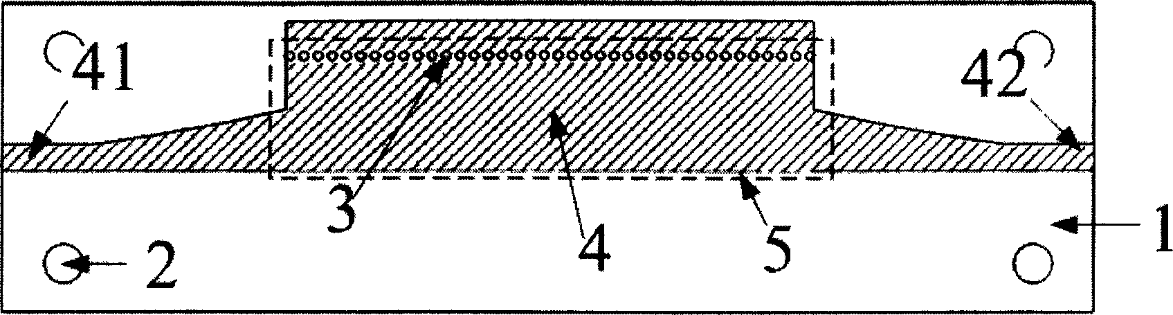
[0012] The half-mode substrate integrated waveguide of the present invention relates to a half-mode substrate integrated waveguide (HMSIW) waveguide structure of millimeter wave and microwave devices, including a dielectric substrate 1 provided with a metal patch, and a row of Periodically arranged metallized holes 3 for connection, the diameter of the metallized through hole is 0.5 mm, and the distance between the centers of adjacent metallized through holes is 0.8 mm; The distance between the edges 5 is 6.5 mm. The input port 41 and the output port 42 are input and output ports, respectively. The above-mentioned metallized through hole is to open a through hole on the dielectric substrate, set a metal sleeve on the inner wall of the through hole and connect the metal sleeve with the metal patches covering both sides of the dielectric substrate.


PUM


Abstract

The invention discloses a half-mold substrate integrated wave (HMSIW), whose two surfaces contains positive metal paster and back metal paster separately, wherein the rectangle wave (4) is composed of positive metal paste on the dielectric substrate (1), whose two ends are input port (41) and output port (42); a row of connecting metal hole (3) is set on the rectangle part of wave (4) middle segment; the metal through-hole (2) is set on four corners of dielectric substrate (1) to fix, which contains metal case in the inner wall of through-hole in connection with metal paster.

Description

technical field [0001] The invention relates to a millimeter wave and microwave waveguide structure, in particular to a half-mode substrate integrated waveguide (HMSIW). Background technique [0002] In the existing design of millimeter-wave and microwave passive devices, the rectangular waveguide has been widely used as a waveguide structure with excellent performance. avoid. The substrate-integrated waveguide (SIW) that has emerged in the past few years can be processed by a standard printed circuit board (PCB) process while maintaining the waveguide characteristics similar to the rectangular waveguide. Significant improvements have been made in size, size, and integration with planar circuits. However, the traditional substrate-integrated waveguide (SIW) has a relatively large size weakness in the lower microwave frequency band (such as X-band and Ku-band), which will lead to infinite circuit board area when designing delicate microwave circuits. This increases the siz...

Claims


Application Information

Patent Timeline
Patent Type & Authority Applications(China)
IPC IPC(8): H01P3/16
Inventor 洪伟刘冰
Owner SOUTHEAST UNIV
Why Eureka
Try Eureka