Printed wiring board fabrication method, printed wiring board photomask, and program for creating a photomask
A technology of printed circuit board and manufacturing method, which is applied in the direction of printed circuit manufacturing, printed circuit making wiring diagram, printed circuit, etc., can solve the problem of unsuitable wiring pattern and the like
- Summary
- Abstract
- Description
- Claims
- Application Information
AI Technical Summary
Problems solved by technology
Method used
Image

Examples
Embodiment approach 1
[0066] First, a method of manufacturing a printed wiring board according to the present invention will be described.
[0067] The substrate of the printed circuit board is made of insulating resin such as glass fiber epoxy resin and paper phenolic resin. A metal foil such as copper foil is formed on the surface of the substrate. Then the dry film photoresist layer is pasted on the metal foil, overlapped with the photomask, and the resist layer is formed by irradiating ultraviolet rays. Then, the portion not covered with the resist layer is etched with an etchant. Then, the resist layer is removed, a wiring pattern is formed, and finally, a printed circuit board is produced.
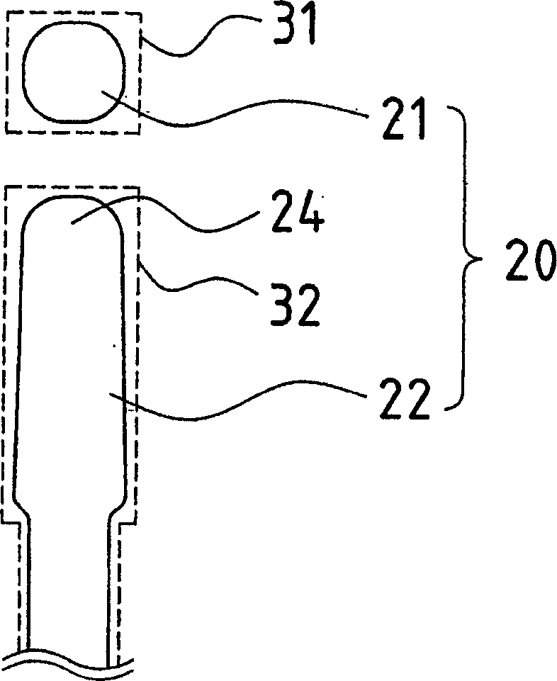
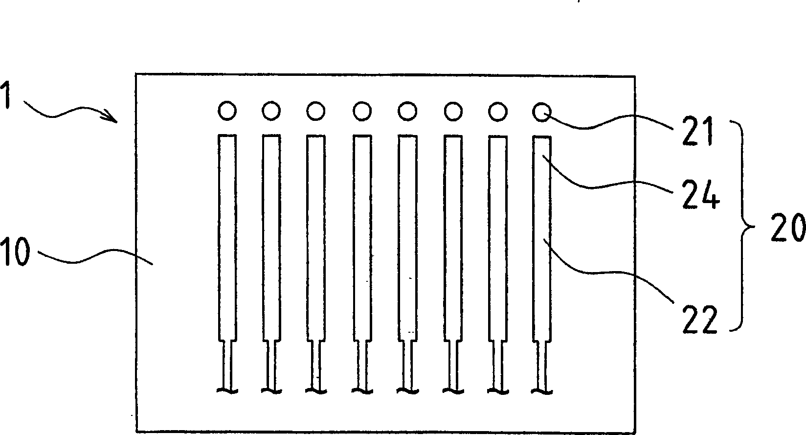
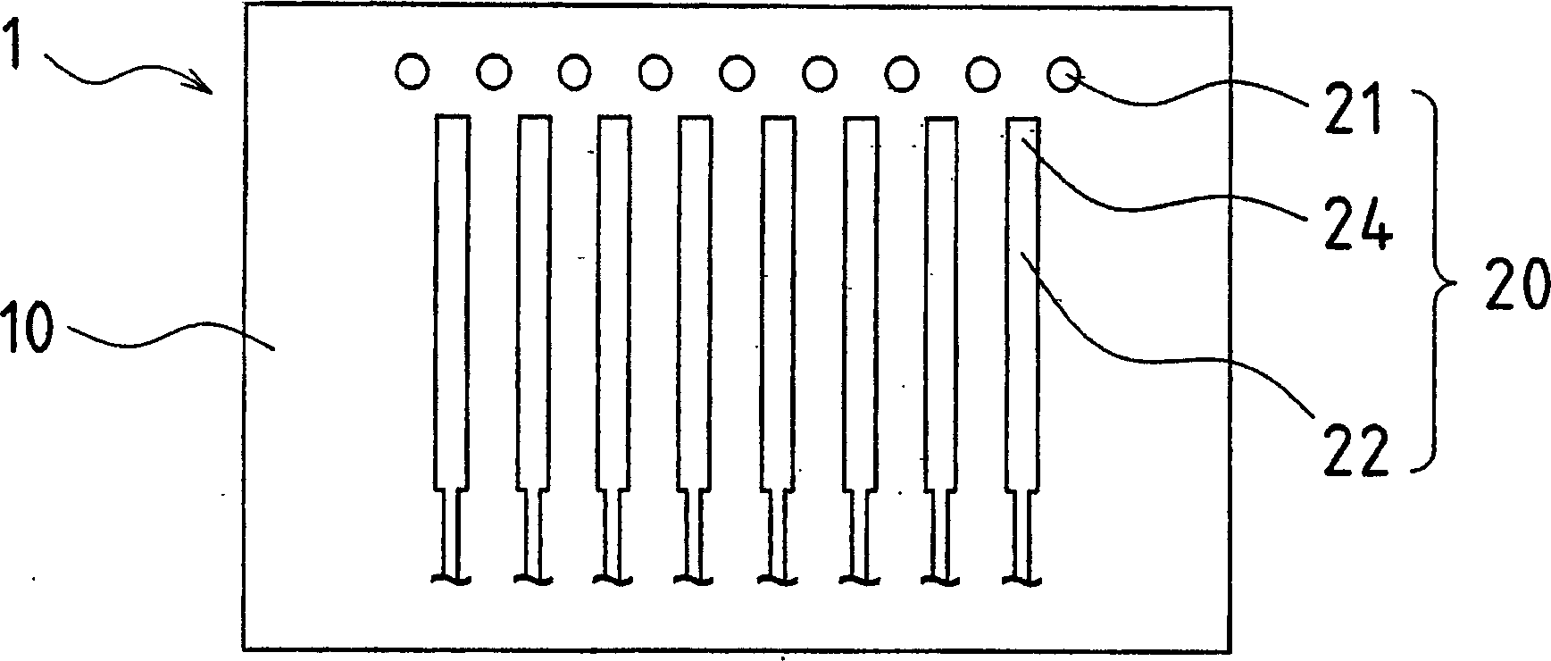
[0068] The wiring pattern has a circuit pattern constituting a circuit and a dummy pattern not required for constituting the circuit. The circuit pattern has, for example, pads connected to terminals such as semiconductors, terminals connected to other electronic components, leads connected to these pa...
Embodiment approach 2
[0090] Below, refer to Figure 1 to Figure 7 The photomask for printed wiring boards concerning this invention is demonstrated.
[0091] A mask pattern for manufacturing the wiring pattern 20 is formed on the photomask. As described in Embodiment 1, the wiring pattern 20 has a circuit pattern constituting a circuit and a dummy pattern 21 which is unnecessary for constituting the circuit. On the contrary, the mask pattern has a circuit pattern, a circuit mask pattern corresponding to the dummy pattern 21, and a dummy mask pattern.
[0092] When manufacturing the printed wiring board 1, by using such a photomask, a photoresist layer corresponding to the circuit pattern and the dummy pattern 21 can be formed, and the printed wiring board 1 with the circuit pattern and the dummy pattern 21 can be produced.
Embodiment approach 3
[0094] Below, refer to Figure 1 to Figure 7 The photomask creation program according to the present invention will be described.
[0095] The photomask generating program has a circuit block for forming a circuit mask pattern from a circuit pattern constituting a circuit, a dummy block for forming a dummy mask pattern corresponding to the dummy pattern 21, and a synthetic circuit mask pattern and a synthesis of the dummy mask pattern. department.
[0096] The circuit module generates a circuit mask pattern with respect to the circuit pattern input to the photomask generation program.
[0097] The dummy module designs the position and shape where the dummy pattern 21 can be arranged according to the circuit pattern input into the photomask generating program, and generates a corresponding dummy mask pattern according to the designed dummy pattern 21 .
[0098] In addition, the circuit mask pattern and the dummy mask pattern are synthesized by the synthesizing unit to generat...
PUM
 Abstract
Description
Claims
Application Information
 - R&D
- Intellectual Property
- Life Sciences
- Materials
- Tech Scout
- Unparalleled Data Quality
- Higher Quality Content
- 60% Fewer Hallucinations
Browse by: Latest US Patents, China's latest patents, Technical Efficacy Thesaurus, Application Domain, Technology Topic, Popular Technical Reports.
© 2025 PatSnap. All rights reserved.Legal|Privacy policy|Modern Slavery Act Transparency Statement|Sitemap|About US| Contact US: help@patsnap.com