

Method of resin seal moulding electronic component and apparatus therefor
A technology for resin sealing and electronic components, which is applied to electrical components, electric solid devices, circuits, etc., can solve the problems of unsimplified metal mold structure, large amount of resin, uneconomical and other problems, achieve easy metal mold maintenance operations, and suppress waste resin. The effect of easy generation and practical application
- Summary
- Abstract
- Description
- Claims
- Application Information
AI Technical Summary
Problems solved by technology
Method used
Image

Examples
Embodiment 1
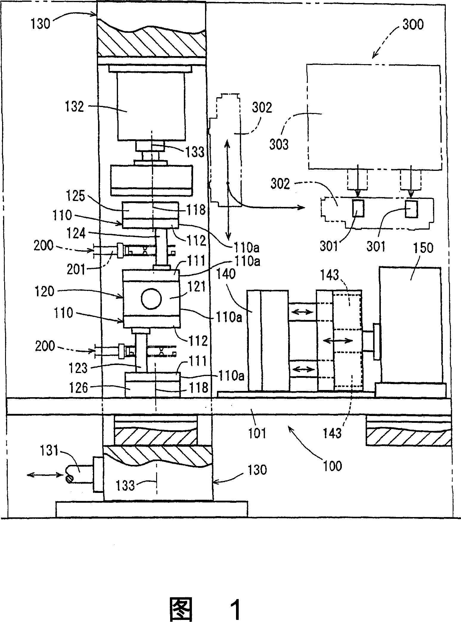
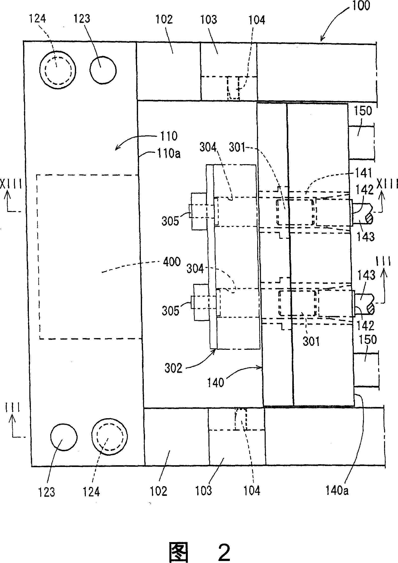
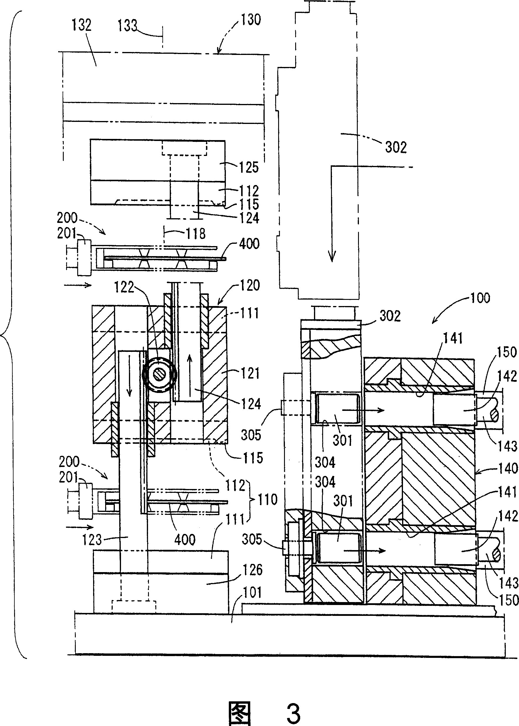
[0078] FIG. 1 schematically shows the overall configuration of a resin sealing molding device.
[0079] This resin sealing and molding apparatus includes: a resin sealing and molding unit 100 for resin sealing and molding an electronic component on a substrate; for transporting and supplying a substrate before resin sealing and molding to a predetermined position described later in the resin sealing and molding unit; a substrate supply and take-out mechanism 200 for taking out the resin-encapsulated substrate from the resin-encapsulation-molding section; Agency 300.
[0080] The resin sealing and molding part 100 includes: a mold 110 for resin sealing and molding electronic components; a mold opening and closing mechanism 120 for opening and closing the mold; A pressurizing mechanism (Japanese: press frame mechanism) 130 for applying the necessary mold clamping pressure to the mold; a feed block (Japanese: pottoblock) 140 arranged on the side of the mold 110 for supplying res...
Embodiment 2
[0133] 15 to 17 show a resin sealing molding apparatus according to another embodiment of the present invention. The difference between this apparatus and the resin sealing molding apparatus of the above-mentioned first embodiment is as follows.
[0134] That is, in the resin sealing molding apparatus of the first embodiment, a resin sealing region (see FIG. 10 ) for resin sealing electronic components is provided on one main surface of a substrate 400, but in FIG. In the resin sealing molding device of this embodiment, there are multiple resin sealing areas (two in the illustration). In addition, the device of this embodiment is similar to the first embodiment in terms of being provided with the feeding chamber 141 for supplying the resin material, the push rod 142 for pressurizing the resin material, and the reciprocating drive mechanism 143 for the push rod, etc. The device of one embodiment is different.
[0135] In addition, the device shown in FIG. 16 has basically the ...
Embodiment 3
[0139] 18 and 19 show a resin sealing and molding apparatus according to another embodiment of the present invention, which is a modified example of the resin sealing and molding apparatus of the second embodiment shown in FIGS. 15 and 16 above.
[0140] Although the number of processed resin-sealed molded products can be increased by using the device of the second embodiment shown in Figure 15 and Figure 16, the device of the third embodiment shown in Figure 18 and Figure 19 can further increase the number of resin-sealed molded products. The number of products processed.
[0141] In the device shown in FIG. 18, the device of the second embodiment shown in FIG. 15 is symmetrically arranged in the figure. In the device shown in FIG. The devices are arranged bilaterally symmetrically in the figure.
[0142] Furthermore, in the apparatus of the third embodiment, the mold clamping pressure described above is applied to each of the molds 110 arranged bilaterally symmetrically. T...
PUM
 Abstract
Description
Claims
Application Information