

Image sensor module package structure
An image sensor and module technology, which is applied in electric solid state devices, semiconductor devices, radiation control devices, etc., can solve problems such as inconvenience and lack of structure in products, avoid optical path interference, and enhance functionality and electrical transmission. The effect of efficiency
- Summary
- Abstract
- Description
- Claims
- Application Information
AI Technical Summary
Problems solved by technology
Method used
Image

Examples
Embodiment Construction
[0051] In order to further explain the technical means and effects of the present invention to achieve the intended purpose of the invention, in conjunction with the accompanying drawings and preferred embodiments, the specific implementation, structure, Features and their functions are described in detail below.
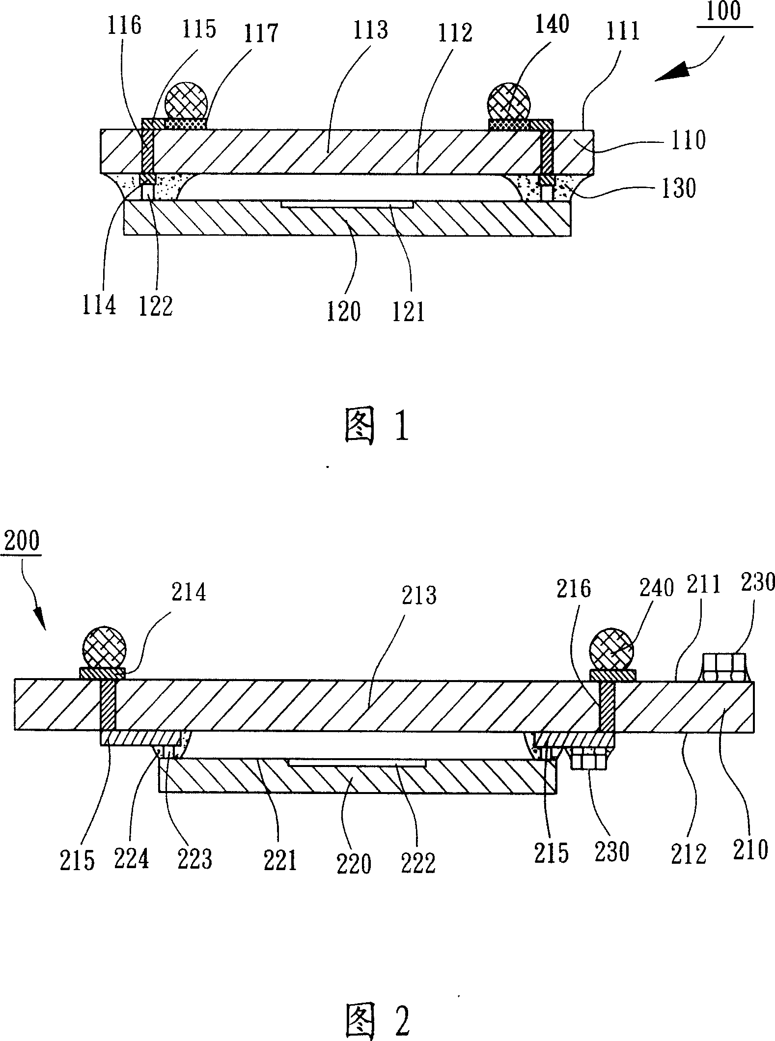
[0052] Please refer to FIG. 2 , which is a schematic cross-sectional view of a first embodiment of the packaging structure of the image sensor module according to the present invention. An image sensor module packaging structure 200 according to the first embodiment of the present invention mainly includes a glass substrate 210, a flip-chip image sensor chip 220 and a plurality of passive components 230, wherein:
[0053] The glass substrate 210 has a first surface 211 and a second surface 212 corresponding to the first surface 211 , and the first surface 211 defines a light incident region 213 . In addition, the glass substrate 210 includes a plurality of connecti...
PUM
 Abstract
Description
Claims
Application Information