

Method for manufacturing semiconductor device
A semiconductor and plasma technology, applied in semiconductor/solid-state device manufacturing, photoengraving process of pattern surface, optics, etc., can solve problems such as total productivity decline and overall process complexity
- Summary
- Abstract
- Description
- Claims
- Application Information
AI Technical Summary
Problems solved by technology
Method used
Image

Examples
Embodiment Construction
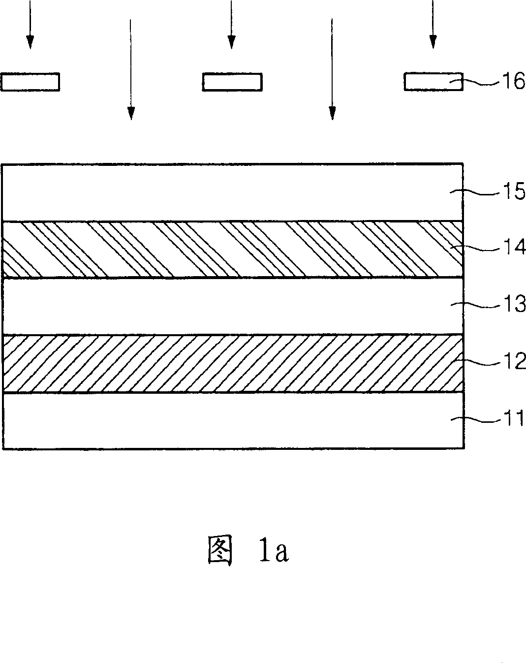
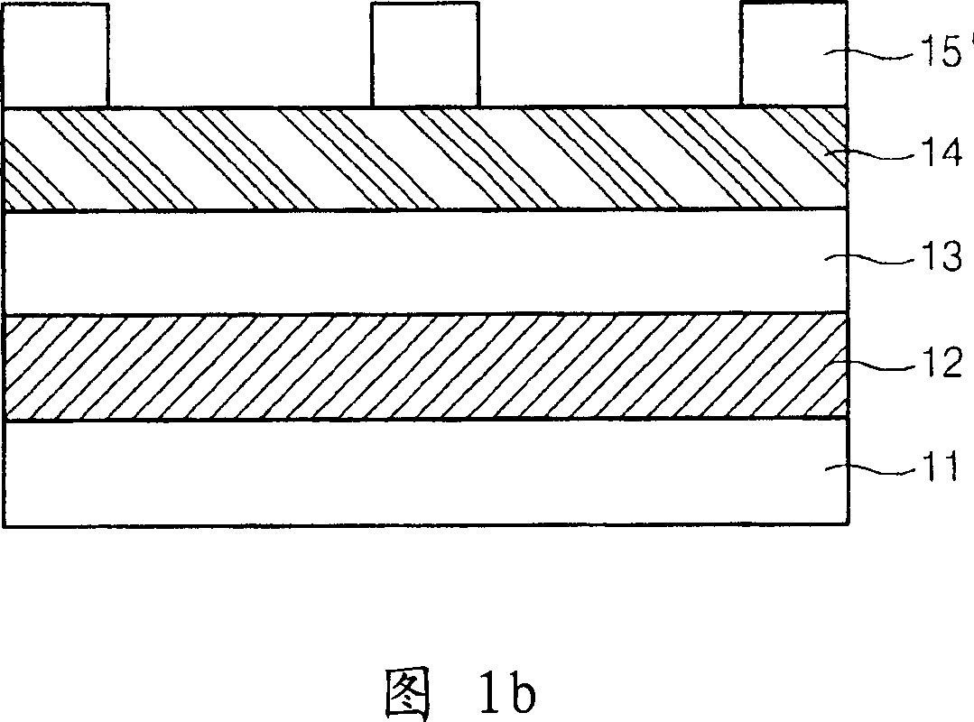
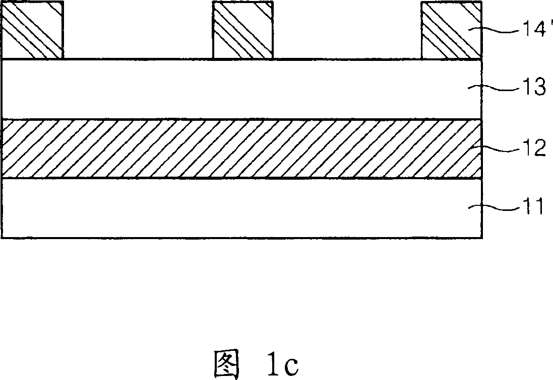
[0047] Disclosed herein is a method of manufacturing a semiconductor device, which includes sequentially forming an underlayer, a hard mask layer, a first antireflection film containing Si, and a first photoresist film on a semiconductor substrate. The method also includes exposing and developing the first photoresist film using a first exposure mask to form a first photoresist pattern, and etching the first photoresist film using the first photoresist pattern as a mask. An anti-reflection film, thereby forming a first anti-reflection pattern. The method also includes performing O on the first anti-reflective pattern 2 plasma treatment, followed by O 2 sequentially forming a second anti-reflection film and a second photoresist film on the plasma-treated first anti-reflection pattern, and exposing and developing alternate regions with respect to the first anti-reflection pattern using a second exposure mask , to form a second photoresist pattern. The method also includes etc...
PUM
 Abstract
Description
Claims
Application Information