Organic electroluminescent device

an electroluminescent device and electroluminescent technology, applied in the direction of electroluminescent light sources, solid-state devices, electric lighting sources, etc., can solve the problems of high power consumption, large volume, heavy weight, etc., and achieve the effect of improving luminous efficiency and luminance properties

Inactive Publication Date: 2009-09-22
SAMSUNG DISPLAY CO LTD
View PDF15 Cites 3 Cited by
  • Summary
  • Abstract
  • Description
  • Claims
  • Application Information

AI Technical Summary

Benefits of technology

[0021]Accordingly, it is an object of the present invention to provide an organic EL device in which luminance properties can be enhanced.
[0026]According to the present invention, a wall surrounding a region where the organic EL layer is formed is comprised of a CVD insulating film of low dielectric constant. Since the surface of the CVD insulating film of low dielectric constant is not damaged due to plasma, the surface treatment of the pixel electrode is performed using O2 plasma to thereby enhance the luminous efficiency and the luminance properties.

Problems solved by technology

The CRT, however, has some disadvantages such as a heavy weight, a large volume and high power consumption.
However, When the metal electrode is formed above the organic insulating film, the lifting of the metal electrode may be caused due to a poor adhesion of the organic insulating film.
This is because the high polymers of the organic insulating film are easily damaged due to the plasma.
That is, when the surface treatment of the plasma electrode is performed using O2 plasma, the surface of the wall is damaged so that the organic insulating film is coated on the contact region to increase a contact resistance and deteriorate the device performance.
Accordingly, in case that the wall is formed of the organic insulating film, the surface treatment process of the pixel electrode cannot be used to thereby deteriorate luminance properties of the organic EL element.

Method used


Image

  • Organic electroluminescent device
  • Organic electroluminescent device
  • Organic electroluminescent device

Examples


first embodiment

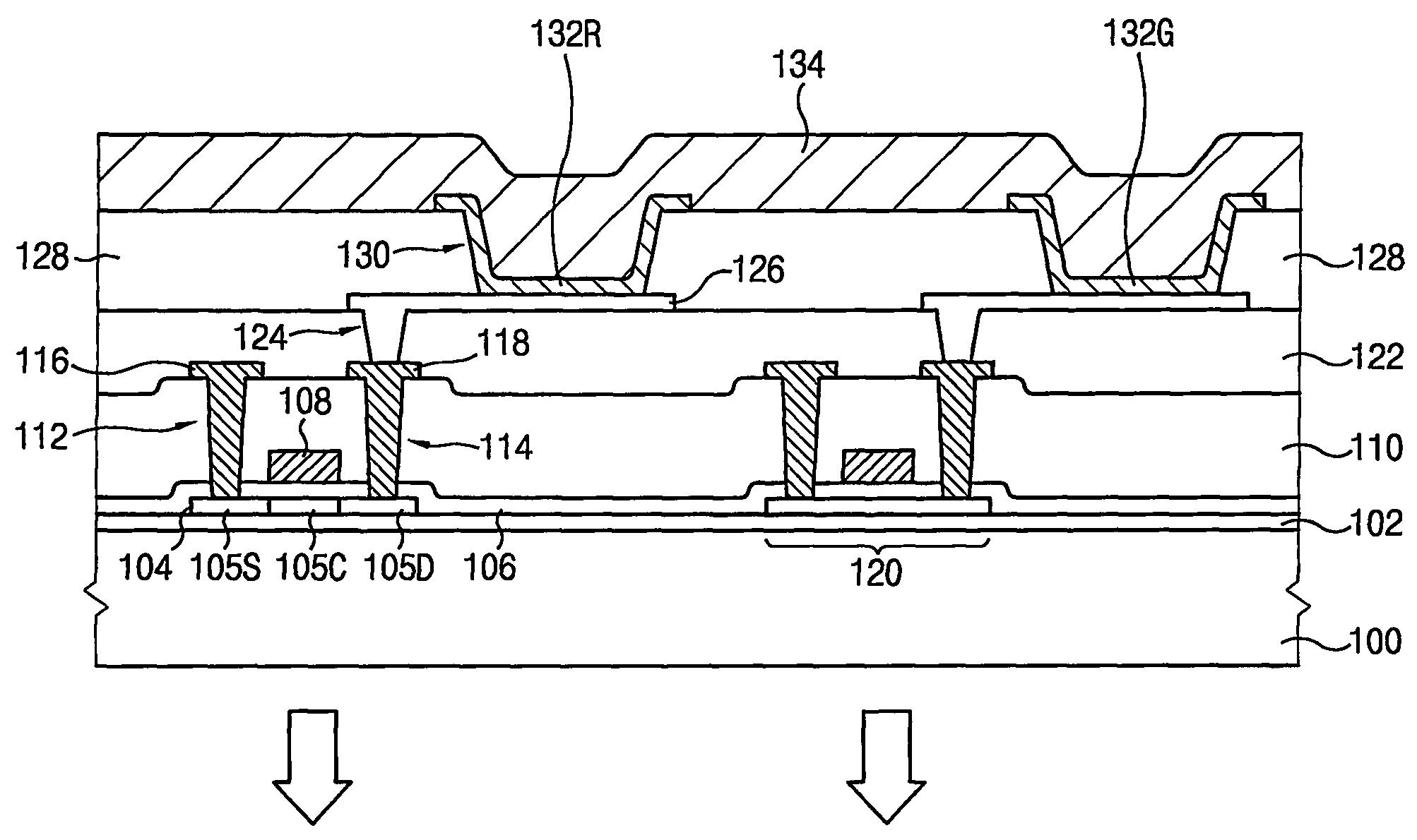
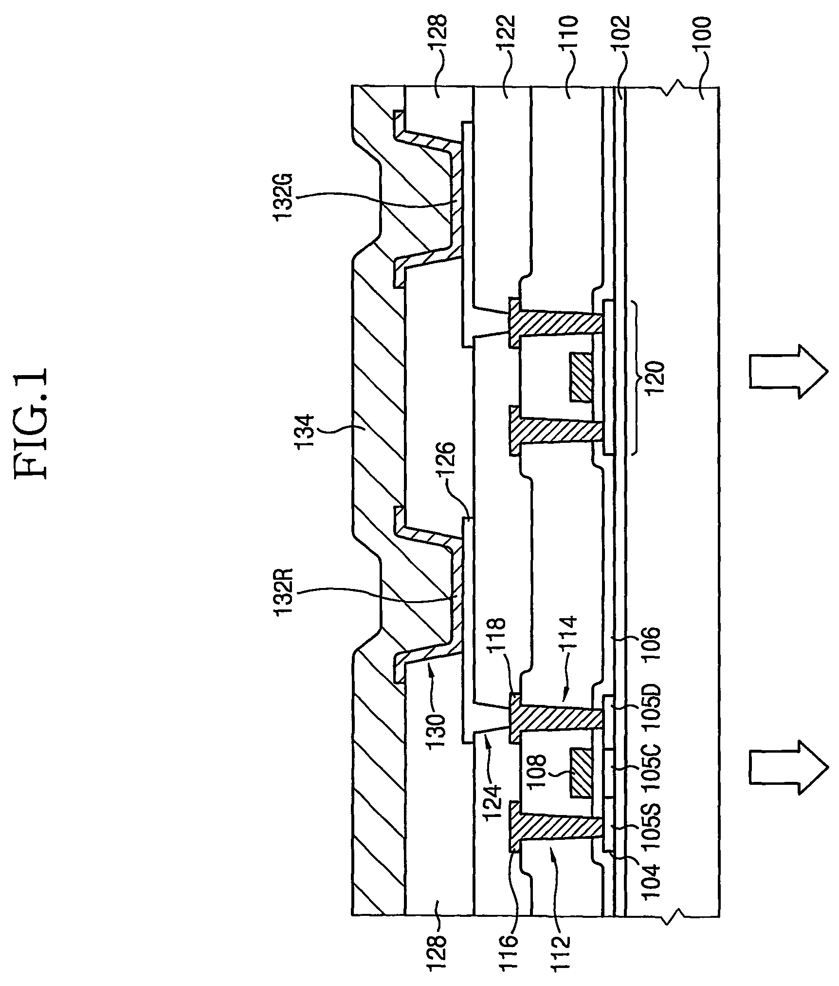
[0035]FIG. 1 is a cross-sectional view of an active matrix type organic EL device in accordance with the present invention.

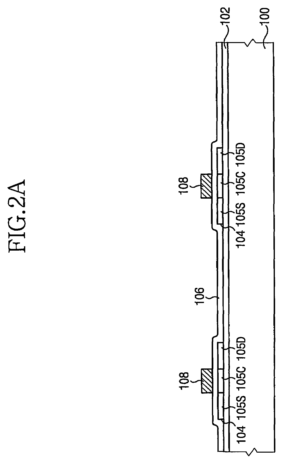
[0036]Referring to FIG. 1, a blocking layer 102 comprised of silicon oxide is formed on the entire surface of a transparent insulating substrate 100 such as glass, quartz, or sapphire. The blocking layer 102 may be skipped, but it is preferred to form the blocking layer 102 in order to prevent impurities in the substrate 100 penetrating into a silicon film during a subsequent crystallization process for an amorphous silicon film.

[0037]On the blocking layer 102, there are formed thin film transistors 120. The thin film transistor 120 includes an active pattern 104, a gate electrode 108 and source / drain electrode 116 and 118. Specifically, polycrystalline active patterns 104 are formed on the blocking layer 102. A gate insulating film 106 comprised of silicon nitride or silicon oxide is formed on the active patterns 104 and the blocking layer 102. Gate electrodes ...

second embodiment

[0065]FIG. 3 is a cross-sectional view of a passive matrix type organic EL device in accordance with the present invention.

[0066]Referring to FIG. 3, first electrodes (i.e., anode electrodes) 210 comprised of a transparent conductive film such as ITO are formed on a transparent insulating substrate 200 such as glass, quartz or sapphire. The first electrodes 210 are formed in a shape of stripe extending a first direction.

[0067]Having openings 240 exposing each of the first electrodes 210, a CVD insulating film 218 of low dielectric constant, e.g., SiOC film is formed on the first electrodes 210 and the substrate 200. Preferably, the CVD insulating film 218 of low dielectric constant has a dielectric constant below 3.5 in order to suppress the formation of a coupling capacitance between the first electrode 210 and a second electrode for a cathode, and is formed to a thickness of 1 um or more.

[0068]The CVD insulating film 218 of low dielectric constant serves as a wall surrounding a re...


PUM


Abstract

Disclosed is an organic electroluminescent (EL) device for enhancing the luminous efficiency. A first electrode is formed on a substrate. A CVD insulating film of low dielectric constant having an opening exposing the first electrode is formed on the first electrode and the substrate. An organic EL layer and a second electrode are sequentially stacked on the opening. A wall surrounding a region of the organic EL layer is formed of the CVD insulating film of low dielectric constant, the surface treatment of the pixel electrode can be performed using O2 plasma enhance luminance properties.

Description

CROSS-REFERENCE TO RELATED APPLICATION[0001]This application is a national phase application of PCT / KR02 / 02418 filed on Dec. 24, 2002, and claims priority thereto under 35 USC 371. PCT / KR02 / 02418, in turn, claims priority from Korean Application No. 10-2002-0033326 filed on Jun. 14, 2002, the content of which is incorporated by reference herein in its entirety.Technical Field[0002]The present invention relates to an organic electroluminescent (EL) device, and more particularly, to an organic EL device in which a CVD insulating film of low dielectric constant is used to enhance the luminous efficiency.Background Art[0003]In the information society of these days, electronic display devices are more important as information transmission media and various electronic display devices are widely applied for industrial apparatus or home appliances. Such electronic display devices are being continuously improved to have new appropriate functions for various demands of the information society...

Claims


Application Information

Patent Timeline
Patent Type & Authority Patents(United States)
IPC IPC(8): H01L29/227H01L29/04H01L21/316H05B33/22H01L27/32H01L51/50H05B33/00H05B33/10H05B33/12
CPCH01L27/3283H01L27/3246H01L21/31633H01L51/5206H10K59/122H10K59/173H01L21/02126H10K59/80515H10K59/8051H05B33/00H10K50/81
Inventor CHUNG, JIN-KOOCHOI, BEOM-RAKCHOI, JOON-HOOKIM, SANG-GABCHOE, HEE-HWAN
Owner SAMSUNG DISPLAY CO LTD
Why Eureka
Try Eureka