Light emitting element, method for manufacturing same, and light emitting device

a technology of light-emitting elements and manufacturing methods, which is applied in the direction of electrical devices, semiconductor devices, organic semiconductor devices, etc., can solve the problems of short operating life, uneven brightness on the light-emitting surface, and inability to ascertain the above-described problems and findings, so as to prolong the operating life of the element and improve the light-emitting property.

Active Publication Date: 2013-05-30
JOLED INC
View PDF3 Cites 31 Cited by
  • Summary
  • Abstract
  • Description
  • Claims
  • Application Information

AI Technical Summary

Benefits of technology

[0011]However, even if the metal oxide is used for forming the charge-injection / transport layer as described above, it is still necessary to further improve the light-emitting property. Also, it is necessary to further lengthen an operating life of the element.
[0012]One non-limiting and exemplary embodiment provides a light-emitter, a method of manufacturing the same and a light-emitting device. Here, the light-emitter has a high light-emitting property and a long operating life even if the metal oxide is used for forming the charge-injection / transport layer.
[0014]With the stated structure, an upper peripheral edge of the recess included in the charge-injection / transport layer is covered with a portion of a bank. Therefore, it is possible to suppress the electrical field from being concentrated in the upper peripheral edge of the recess when light is emitted. Therefore, the light-emitter pertaining to one aspect of the present invention has a light-emitting property and an operating life that have been further improved.

Problems solved by technology

As a result, current locally flows to the organic light-emitting layer 905 in some cases, which results in uneven brightness on a light-emitting surface and a short operating life due to a local deterioration.
Also, the above-described problems and findings had not been ascertained.
Therefore, these problems and findings have technical significance.
Such leak current causes a variety of problems such as increased power consumption.
Therefore, there is a problem that the light generated by the light-emitting layer is absorbed by the charge-injection / transport layer absorbs before being emitted to the outside, which leads to the degradation of the luminous efficiency.
There is another problem.

Method used


Image

  • Light emitting element, method for manufacturing same, and light emitting device
  • Light emitting element, method for manufacturing same, and light emitting device
  • Light emitting element, method for manufacturing same, and light emitting device

Examples


first embodiment

1. Overall Structure of Display Device 1

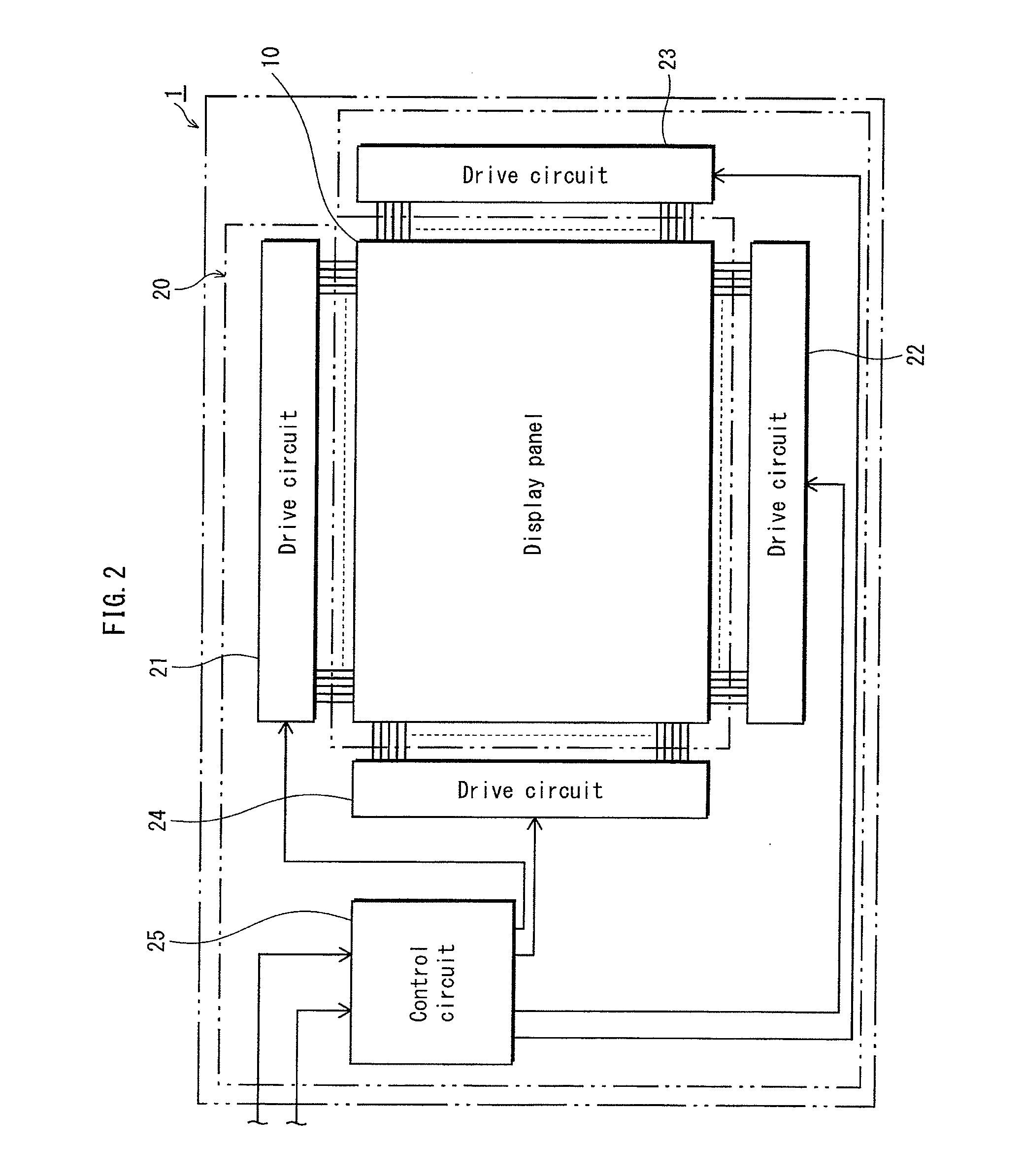
[0069]The overall structure of the display device 1 pertaining to a first embodiment is described with use of FIG. 2.

[0070]As shown in FIG. 2, the display device 1 includes a display panel 10 and a drive control unit 20 that is connected to the display panel 10. The display panel unit 10 is an organic EL panel that uses the phenomenon of electroluminescence occurring in organic material and is composed of an array of a plurality of organic EL elements.

[0071]The drive control unit 20 is composed of four drive circuits 21-24 and a control circuit 25.

[0072]Note that in an actual display device 1, the placement of the drive control unit 20 with respect to the display panel unit 10 is not limited in this way.

2. Structure of Display Panel 10

[0073]The following describes the structure of the display panel 10 with use of FIG. 3 and FIG. 4.

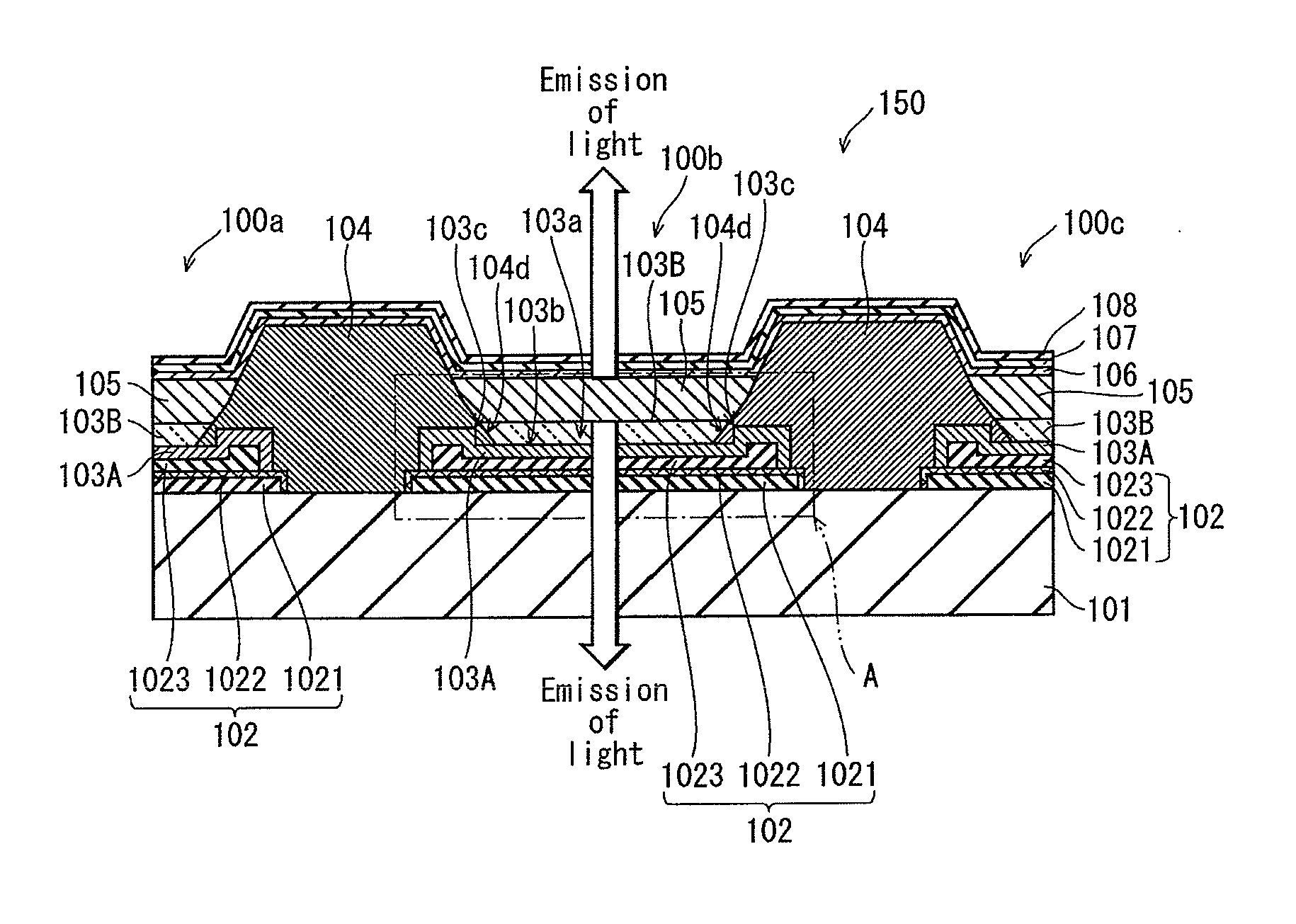
[0074]As shown in FIG. 3, the display panel 10 has a structure in which organic EL elements 100a, 100b and 100c ar...

second embodiment

[0147]The following describes a structure of an organic EL element 110 pertaining to a second embodiment, with reference to FIG. 9. Note that elements of the organic EL elements 100a, 100b and 100c that are the same as the elements thereof in the first embodiment have the same reference numerals in FIG. 9, and descriptions thereof are omitted.

[0148]As shown in FIG. 9, the organic EL element 110 pertaining to the present embodiment is different from each of the organic EL elements 100a, 100b and 100c in the first embodiment in a form of an anode metal layer 1123 of an anode 112 and a form of a hole injection transport layer 113 formed on the anode metal layer 1123. Specifically, in the organic El element 110, the anode metal layer 1123 is formed so as to cover side surfaces 1022f of the ITO layer 1022, and bottom surfaces of end portions of the hole injection transport layer 113 are in contact with the principal surface of the substrate 101.

[0149]Note that, in the organic EL element ...

third embodiment

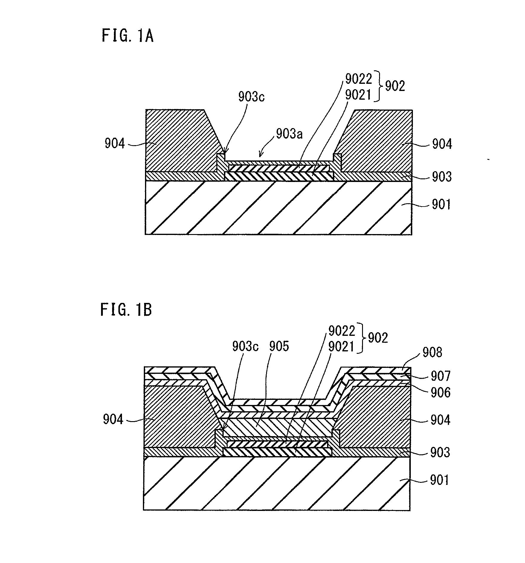
[0151]A description is given of a structure of an organic EL element 120 pertaining to a third embodiment, with reference to FIG. 10. Also, a description is given of characteristics of a method of manufacturing the organic EL element 120, with reference to FIGS. 11A, 11B and 11C. Elements that are the same as elements of the organic EL elements 100a, 100b and 100c pertaining to the first embodiment have the same reference numerals in FIG. 10 and FIGS. 11A, 11B and 11C. Therefore, the descriptions thereof are omitted.

[0152]As shown in FIG. 10, the organic EL element 120 pertaining to the present embodiment is different from the organic EL elements 100a, 100b and 100c pertaining to the first embodiment in a form of an anode 122. Specifically, in the present embodiment, an anode base layer 1221 of the anode 122 and an ITO layer 1222 that is layered on the anode base layer 1221 have the same width as the hole injection transport layer 103.

[0153]The organic EL element 120 pertaining to t...


PUM


Abstract

Organic light-emitting elements each have the following structure: a transparent anode, a functional layer including a charge injection layer and an organic light-emitting layer, and a transparent cathode are layered on a substrate in the stated order; a bank defines a formation area of the organic light-emitting layer; the charge injection layer is a metal oxide layer formed by oxidizing an upper surface portion of the anode composed of the metal layer, and a portion of the charge injection layer that is positioned under the area is depressed so as to form a recess; and the upper peripheral edge of the recess is covered with a covering portion of the bank.

Description

CROSS REFERENCE TO RELATED APPLICATIONS[0001]This is a continuation application of PCT Application No. PCT / JP2010 / 004957 filed Aug. 6, 2010, designating the United States of America, the disclosure of which, including the specification, drawings and claims, is incorporated herein by reference in its entirety.TECHNICAL FIELD[0002]The present disclosure relates to a light-emitter that takes advantage of an electroluminescence phenomenon of an organic material, a method of manufacturing the same and a light-emitting device.DESCRIPTION OF THE RELATED ART[0003]In recent years, an organic electroluminescence element (hereinafter referred to as “organic EL element”) has been studied and developed. The organic EL element is a light-emitter that takes advantage of an electroluminescence phenomenon of an organic material. The organic EL element has a structure in which an organic light-emitting layer is positioned between an anode and a cathode. A hole is injected from the anode and an electr...

Claims


Application Information

Patent Timeline
Patent Type & Authority Applications(United States)
IPC IPC(8): H01L33/42
CPCH01L33/42H01L51/5088H01L2251/5323H01L27/3246H01L27/3283H10K59/122H10K59/173H10K50/17H10K2102/3031
Inventor TAKEUCHI, TAKAYUKINISHIYAMA, SEIJI
Owner JOLED INC
Why Eureka
Try Eureka