GaN based semiconductor light emitting device and lamp

a light-emitting device and semiconductor technology, applied in semiconductor devices, semiconductor/solid-state device testing/measurement, electrical equipment, etc., can solve the problems of large load applied reduced internal quantum efficiency, and large damage to the semiconductor layer, so as to achieve the effect of stably forming a buffer layer, forming the buffer layer even more stably, and high crystallinity

Active Publication Date: 2011-06-28
TOYODA GOSEI CO LTD
View PDF35 Cites 30 Cited by
  • Summary
  • Abstract
  • Description
  • Claims
  • Application Information

AI Technical Summary

Benefits of technology

[0037]According to the light emitting device of the present invention, it is possible to stably form a buffer layer since the buffer layer is formed on a sapphire substrate, in which an uneven pattern composed of a convex shape or a concave shape is formed, by a sputtering method. Moreover, it is possible to form the buffer layer even more stably when an apparatus used in the sputtering method is equipped with a pivoted magnetron magnetic circuit.
[0038]By stably forming a buffer layer, it will be possible to grow a GaN based semiconductor layer having high crystallinity, and thus it will be possible to form a GaN based semiconductor layer that includes a light emitting layer with excellent light emitting properties.
[0039]Therefore, a light emitting device which is excellent in terms of the light emitting properties of the light emitting layer and the light emission efficiency is obtained.
[0040]In addition, according to the method for producing a light emitting device of the present invention, it will be possible to produce a light emitting device which is excellent in terms of the light emitting properties of the light emitting layer and the light emission efficiency due to the configurations described above.
[0041]In addition, the lamp of the present invention has excellent light emitting properties since the light emitting device of the present invention is used therein.

Problems solved by technology

However, in the light emitting device disclosed in Patent Document 1, since a semiconductor material is processed, a large load is applied to the semiconductor layer, and the semiconductor layer is greatly damaged.
For this reason, although the light emission efficiency improves, the internal quantum efficiency reduces, and thus it is impossible to increase the light emission intensity, which is a problem.
Accordingly, it is difficult to grow a compound semiconductor stably, which is a problem.[Patent Document 1] Japanese Patent Publication No. 2836687[Patent Document 2] Japanese Unexamined Patent Application, First Publication No. 2005-64492

Method used


Image

  • GaN based semiconductor light emitting device and lamp
  • GaN based semiconductor light emitting device and lamp
  • GaN based semiconductor light emitting device and lamp

Examples


example 1

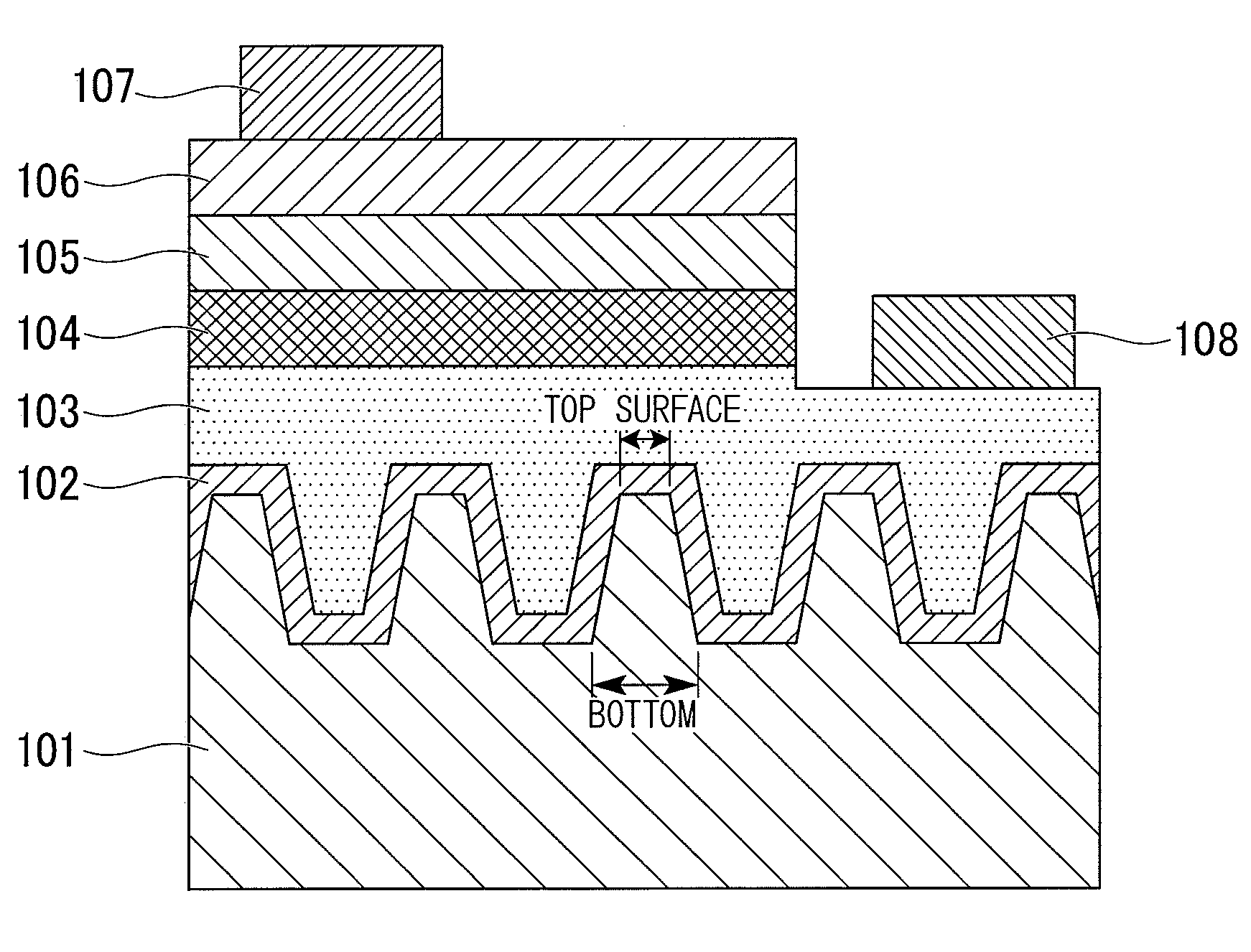
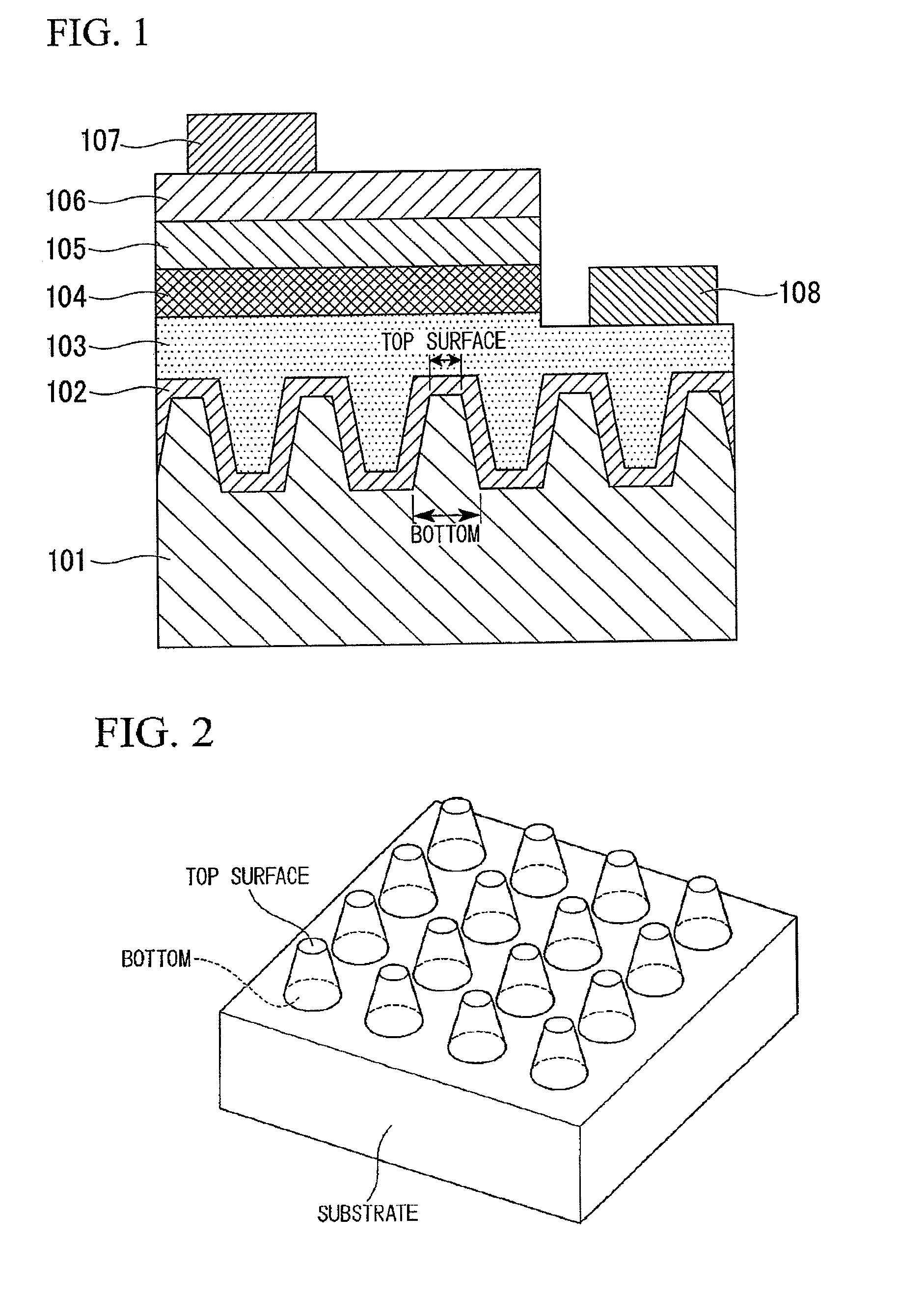
[0124]FIG. 1 is a cross sectional diagram schematically showing a gallium nitride based compound semiconductor light emitting device produced in the present Experimental example.

(Method for Producing Sapphire Substrate with Uneven Pattern Composed of Convex Shape or Concave Shape)

[0125]A sapphire single crystal was used for a substrate. A concave shape was formed on the sapphire single crystal substrate by employing a known photolithography method. BCl3 was used as an etching gas for etching the sapphire single crystal substrate. A truncated cone shape (top dimension: 4 μm, bottom dimension: 2 μm, height: 6 μm, and periodic interval: 8 μm) was formed as the concave shape.
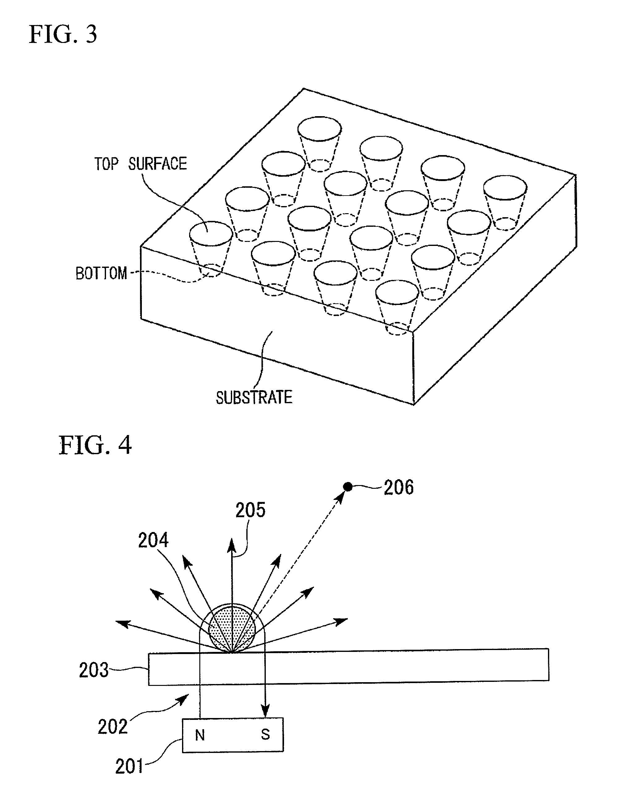
(Sputtering Method)

[0126]AlN was deposited by the RF sputtering method. Al was used as a target and an AlN layer was formed by a process of reactive sputtering with N2. By using the pivoted magnetron magnetic circuit, the layer was formed due to the reciprocating movement (one reciprocating movement in 30 seconds) o...


PUM


Abstract

A method for producing a gallium nitride based compound semiconductor light emitting device which is excellent in terms of the light emitting properties and the light emission efficiency and a lamp is provided. In such a method for producing a gallium nitride based compound semiconductor light emitting device, which is a method for producing a GaN based semiconductor light emitting device having at least a buffer layer, an n-type semiconductor layer, a light emitting layer, and a p-type semiconductor layer on a translucent substrate, on which an uneven pattern composed of a convex shape and a concave shape is formed, the buffer layer is formed by a sputtering method conducted in an apparatus having a pivoted magnetron magnetic circuit and the buffer layer contains AlN, ZnO, Mg, or Hf.

Description

TECHNICAL FIELD[0001]The present invention relates to a light emitting device, and in particular relates to a method for producing a light emitting device that is highly reliable and has excellent light emission efficiency and a lamp that includes the light emitting device produced by employing the method.[0002]Priority is claimed on Japanese Patent Application No. 2006-096340, filed Mar. 31, 2006, the content of which is incorporated herein by reference.BACKGROUND ART[0003]In recent years, a gallium nitride (GaN) based compound semiconductor material which is a nitride based semiconductor has been attracting attention as a semiconductor material for short wavelength light emitting devices. The GaN based compound semiconductor is formed on substrates made of various oxides or group III-V compounds, such as a sapphire single crystal, using a method such as the metal organic chemical vapor deposition method (MOCVD method) and the molecular beam epitaxial method (MBE method).[0004]A co...

Claims


Application Information

Patent Timeline
Patent Type & Authority Patents(United States)
IPC IPC(8): H01L21/66H01L33/12H01L33/22H01L33/24H01L33/32
CPCH01L33/22H01L33/007
Inventor OSAWA, HIROSHISHINOHARA, HIRONAO
Owner TOYODA GOSEI CO LTD
Why Eureka
Try Eureka