Diamond and GaN wafer direct bonding method

A direct bonding, diamond technology, used in electrical components, electrical solid-state devices, semiconductor/solid-state device manufacturing, etc., to achieve the effect of reducing device size and improving radio frequency and power performance

Inactive Publication Date: 2017-05-31
DONGGUAN GUANGXIN INTPROP SERVICES CO LTD +1
View PDF10 Cites 4 Cited by
  • Summary
  • Abstract
  • Description
  • Claims
  • Application Information

AI Technical Summary

Problems solved by technology

However, effective bonding of GaN materials and diamond materials is still a challenging technology. Through technology research and development, it is necessary to increase the bonding rate between GaN materials and diamond materials to meet the high performance of heterogeneous integration. Technical Requirements for GaN Devices

Method used


Image

  • Diamond and GaN wafer direct bonding method

Examples


Embodiment Construction

[0015] In order to make the purpose, technical solutions and advantages of the present invention clearer, the following in conjunction with specific examples, and with reference to the appended figure 1 , to further describe the present invention in detail.

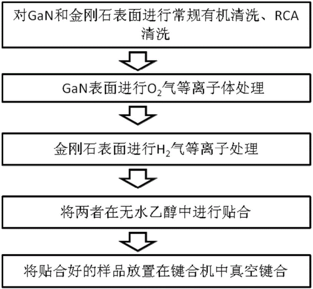
[0016] Such as figure 1 As shown, the present embodiment provides a method for direct bonding of diamond and GaN wafers, the method comprising the following steps: (1) carrying out organic cleaning and RCA cleaning on the surface of diamond and GaN; (2) cleaning the surface of GaN carry out O 2 Gas plasma treatment; (3) H2 gas plasma treatment is carried out on the diamond surface; (4) The two are bonded in absolute ethanol;

[0017] (5) Place the bonded samples in a bonding machine for bonding under a high-temperature vacuum environment.

[0018] In the present embodiment, the processing condition of carrying out oxygen plasma treatment to GaN surface in step (2) is: O 2 =30sccm, RF power is 50W, pressure is 2Par. T...


PUM


Abstract

The invention discloses a damond and GaN wafer direct bonding method. The method comprises the following steps that: (1) organic cleaning and RCA cleaning are performed on a diamond surface and a GaN surface; (2) O2 plasma treatment is performed on the GaN surface; (3) H2 plasma treatment is performed on the diamond surface; (4) the treated diamond surface and the GaN surface are attached to each other in absolute ethyl alcohol; and (5) an obtained attached sample is arranged in a bonding machine so as to be subjected to bonding under high vacuum environment.

Description

technical field [0001] The invention relates to the technical field of semiconductor integrated circuit manufacturing, in particular to a method for direct bonding between diamond and gallium nitride, which is applied to the performance improvement technology of third-generation semiconductor devices with high power and high breakdown voltage. Background technique [0002] Compared with silicon, gallium arsenide and indium phosphide semiconductor materials, gallium nitride semiconductor materials are called third-generation semiconductor materials. It has excellent inherent high breakdown field strength and high saturation drift speed under high field strength. The characteristics determine that it will occupy a leading position in future high-frequency, high-temperature, and ultra-high-power devices. GaN material is a wide bandgap (3.49eV) semiconductor, which has fast electron saturation drift (2.7×10 7 cm / s), high critical breakdown field strength (3.3MV / cm), high two-di...

Claims


Application Information

Patent Timeline
IPC IPC(8): H01L21/60
CPCH01L24/50
Inventor 刘丽蓉王勇丁超
Owner DONGGUAN GUANGXIN INTPROP SERVICES CO LTD
Why Eureka
Try Eureka