Memory bitcell with column select

a memory bitcell and column select technology, applied in the field of memory circuits, can solve the problems of reducing affecting the writability of the column select load, and tensing to add area, so as to improve the column select functionality of the memory circuit, improve the area and power performance, and improve the writability

Active Publication Date: 2018-06-26
ORACLE INT CORP
View PDF15 Cites 1 Cited by
  • Summary
  • Abstract
  • Description
  • Claims
  • Application Information

AI Technical Summary

Benefits of technology

[0003]Among other things, systems and methods are described for improving column selection functionality of memory circuits. Embodiments operate in context of memory bitcells having additional series pass gates (e.g., junction sharing transistors) coupled with a column select signal to form an integrated column select port. Such a column select port can provide each bitcell with column select functionality in a manner that has improved area and power performance over conventional (added NOR or other logic) approaches. However, the added column select port can still tend to add area, add column select load, and degrade writability (e.g., due to certain charge-sharing effects). Some embodiments are described herein for addressing the area and column select load by sharing certain intermediate nodes among multiple, adjacent bitcells. Other embodiments can include additional ground-connected transistors in a manner that improves writability (e.g., and read noise margin) of the bitcell.

Problems solved by technology

However, the added column select port can still tend to add area, add column select load, and degrade writability (e.g., due to certain charge-sharing effects).

Method used


Image

  • Memory bitcell with column select
  • Memory bitcell with column select
  • Memory bitcell with column select

Examples


Embodiment Construction

[0018]In the following description, numerous specific details are set forth to provide a thorough understanding of the present invention. However, one having ordinary skill in the art should recognize that the invention may be practiced without these specific details. In some instances, circuits, structures, and techniques have not been shown in detail to avoid obscuring the present invention.

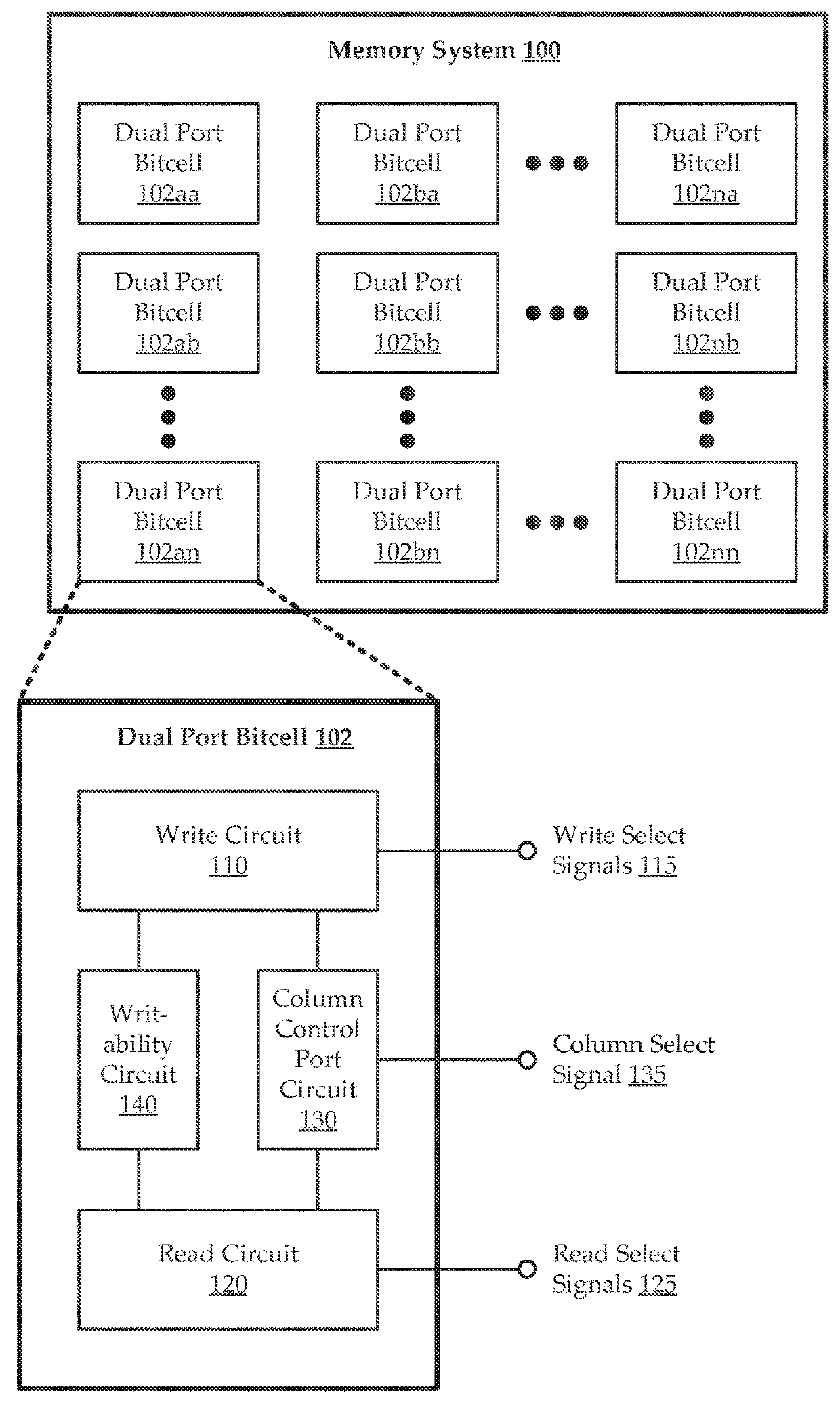
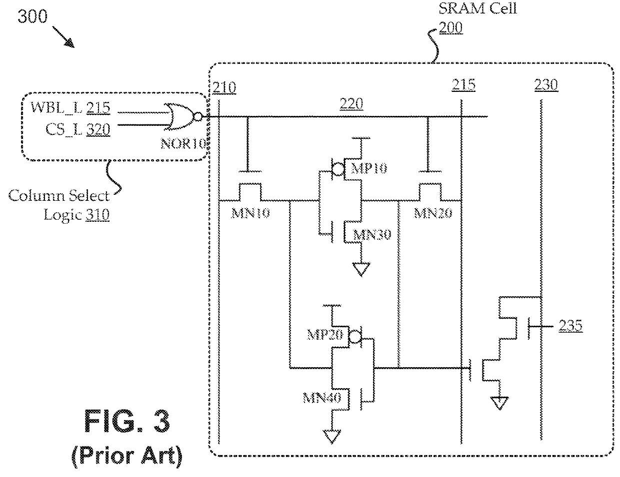
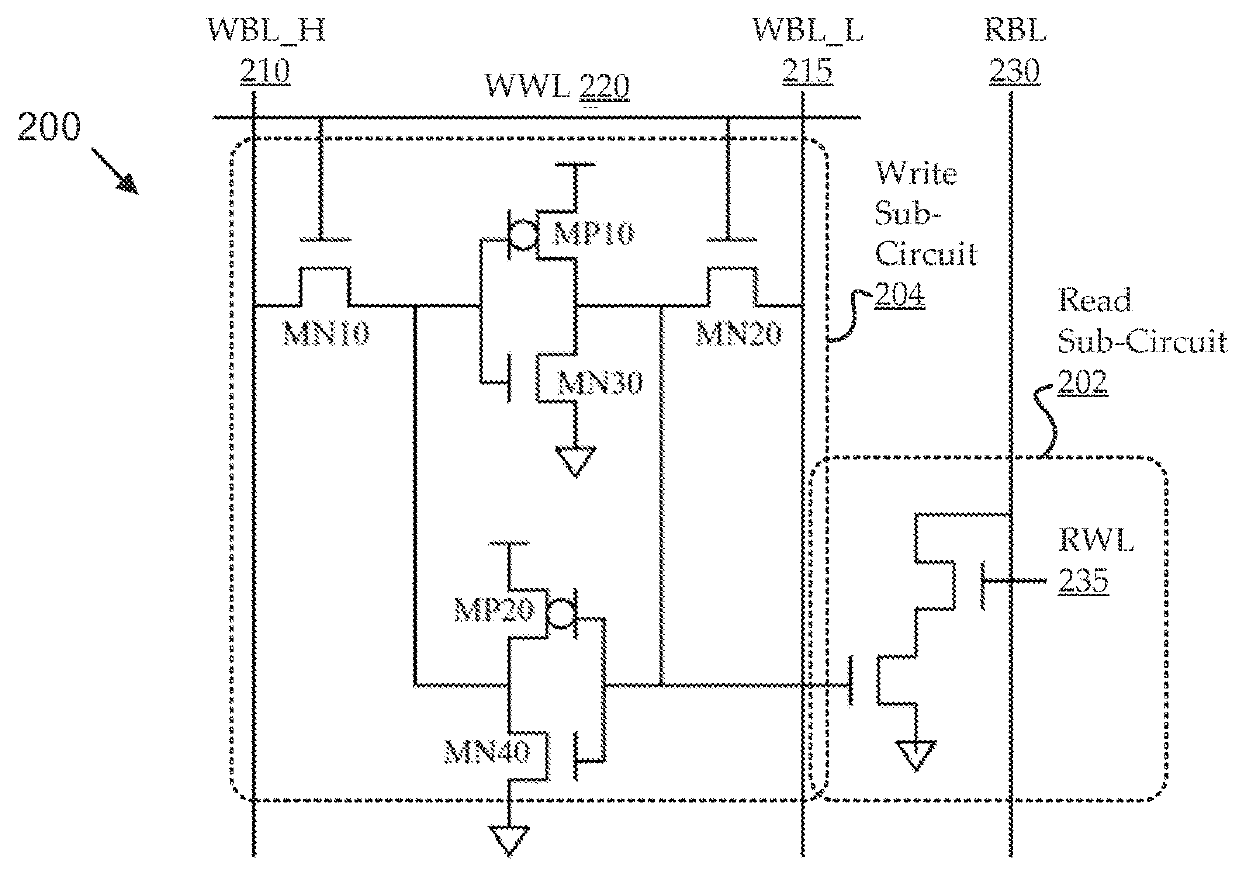
[0019]FIG. 1 shows a simplified block diagram of a memory system 100 and an illustrative dual-port memory bitcells 102, according to various embodiments. Some implementations of the memory system 100 can include semiconductor memory that uses bi-stable latching (e.g., cross-coupled inverters or the like) to store bits in bitcells 102, such as static random access memory (SRAM). The memory system includes a number of bitcells 102, which can be arranged as an array or in any other suitable manner. Embodiments of the bitcells 102 are shown as dual-port bitcells 102, such as bitcells 102 having rea...


PUM


Abstract

Embodiments include systems and methods for improving column selection functionality of memory circuits. Embodiments operate in context of memory bitcells having additional series pass gates (e.g., junction sharing transistors) coupled with a column select signal to form an integrated column select port. Such a column select port can provide each bitcell with column select functionality in a manner that has improved area and power performance over some conventional (added NOR or other logic) approaches. However, the added column select port can still tend to add area, add column select load, and degrade writability (e.g., due to certain charge-sharing effects). Some embodiments are described herein for addressing the area and column select load by sharing certain intermediate nodes among multiple, adjacent bitcells. Other embodiments can include additional ground-connected transistors in a manner that improves writability (e.g., and read noise margin) of the bitcell.

Description

FIELD[0001]Embodiments relate generally to memory circuits, and, more particularly, to dual-port memory bitcell circuits having enhanced column select functionality.BACKGROUND[0002]Typical memory circuits, such as static random access memory (SRAM) circuits, include a number of bitcells that can be written to and read from. Typically, the bitcells are arranged in an array, and individual bitcells can be addressed (for reading or writing) by selecting a corresponding column and row at which the bitcell is located in the array. Conventional bitcell designs typically include integrated row selection ports, but column selection is typically performed using circuitry external to the bitcell. For example, a NOR gate, or other suitable logic, can be added for column selection. Such approaches can have certain limitations, such as increasing area and power consumption of the memory circuit.BRIEF SUMMARY[0003]Among other things, systems and methods are described for improving column selectio...

Claims


Application Information

Patent Timeline
Patent Type & Authority Patents(United States)
IPC IPC(8): G11C11/412G11C11/418G11C11/419G11C7/18
CPCG11C11/419G11C11/418G11C11/412G11C7/18
Inventor KWACK, JINHOCHO, HOYEOLPARK, HEECHOULWON, MYUNG GYOOLABRECQUE, PETERLEE, JUNGYONG
Owner ORACLE INT CORP
Why Eureka
Try Eureka