Vertical trench routing in a substrate

a technology of vertical trenches and substrates, applied in the direction of waveguides, electrical apparatus construction details, waveguide type devices, etc., can solve the problems of circuit design capability or a costly on-board retimer, channel length limitations of conventional pcb routing configurations, and excessive pcb loss

Active Publication Date: 2018-09-18
INTEL CORP
View PDF7 Cites 5 Cited by
  • Summary
  • Abstract
  • Description
  • Claims
  • Application Information

AI Technical Summary

Problems solved by technology

Conventional PCB routing configurations have channel length limitations when used in high speed signaling situations.
A channel length larger than this will experience too much PCB loss or require circuit design capability or a costly on-board retimer, both of which increase the bill of materials (BOM) associated with the platform.

Method used


Image

  • Vertical trench routing in a substrate
  • Vertical trench routing in a substrate
  • Vertical trench routing in a substrate

Examples


Embodiment Construction

[0022]In the following description, numerous details are set forth to provide a more thorough explanation of the present invention. It will be apparent, however, to one skilled in the art, that the present invention may be practiced without these specific details. In other instances, well-known structures and devices are shown in block diagram form, rather than in detail, in order to avoid obscuring the present invention.

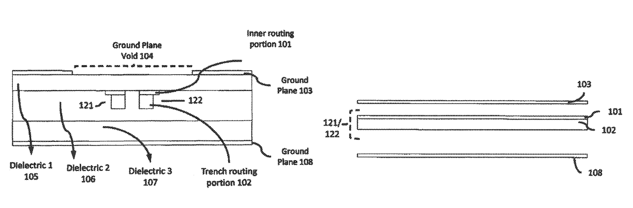
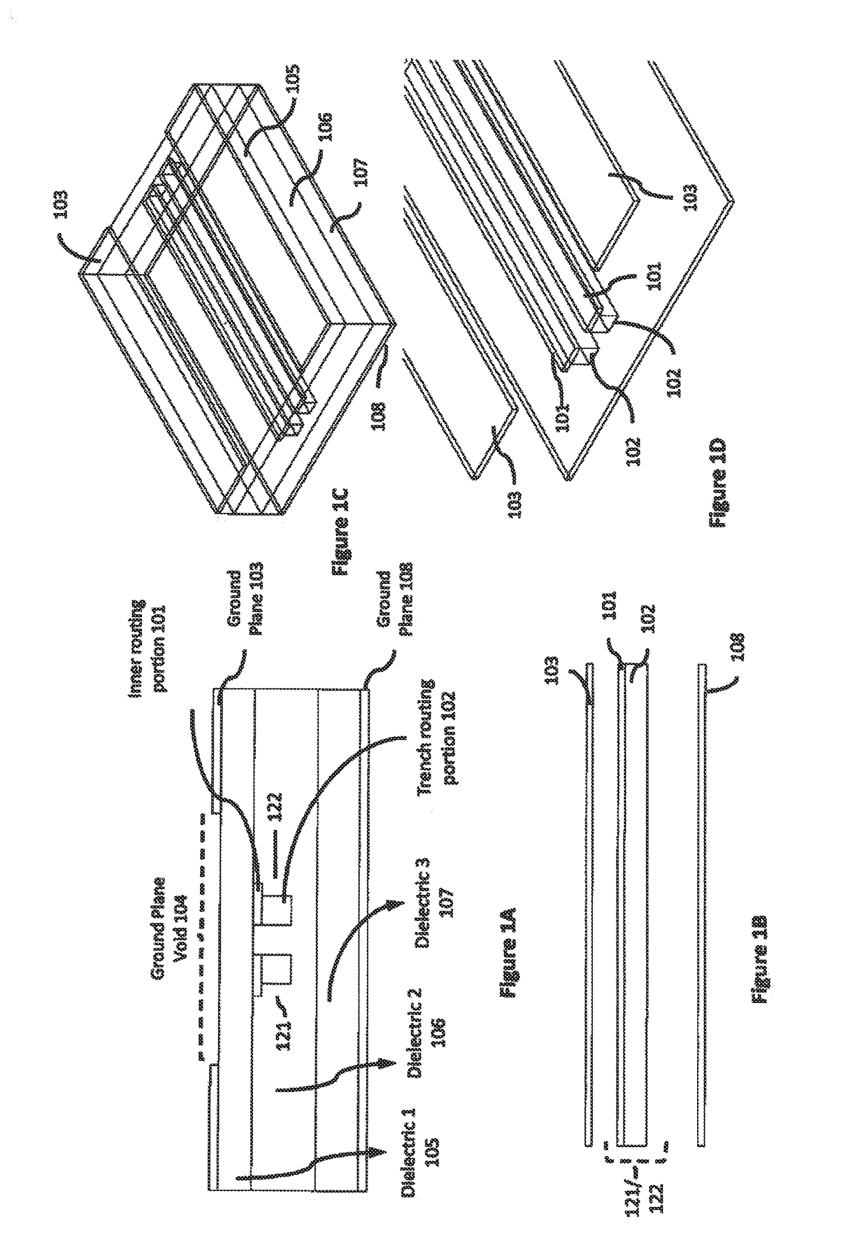
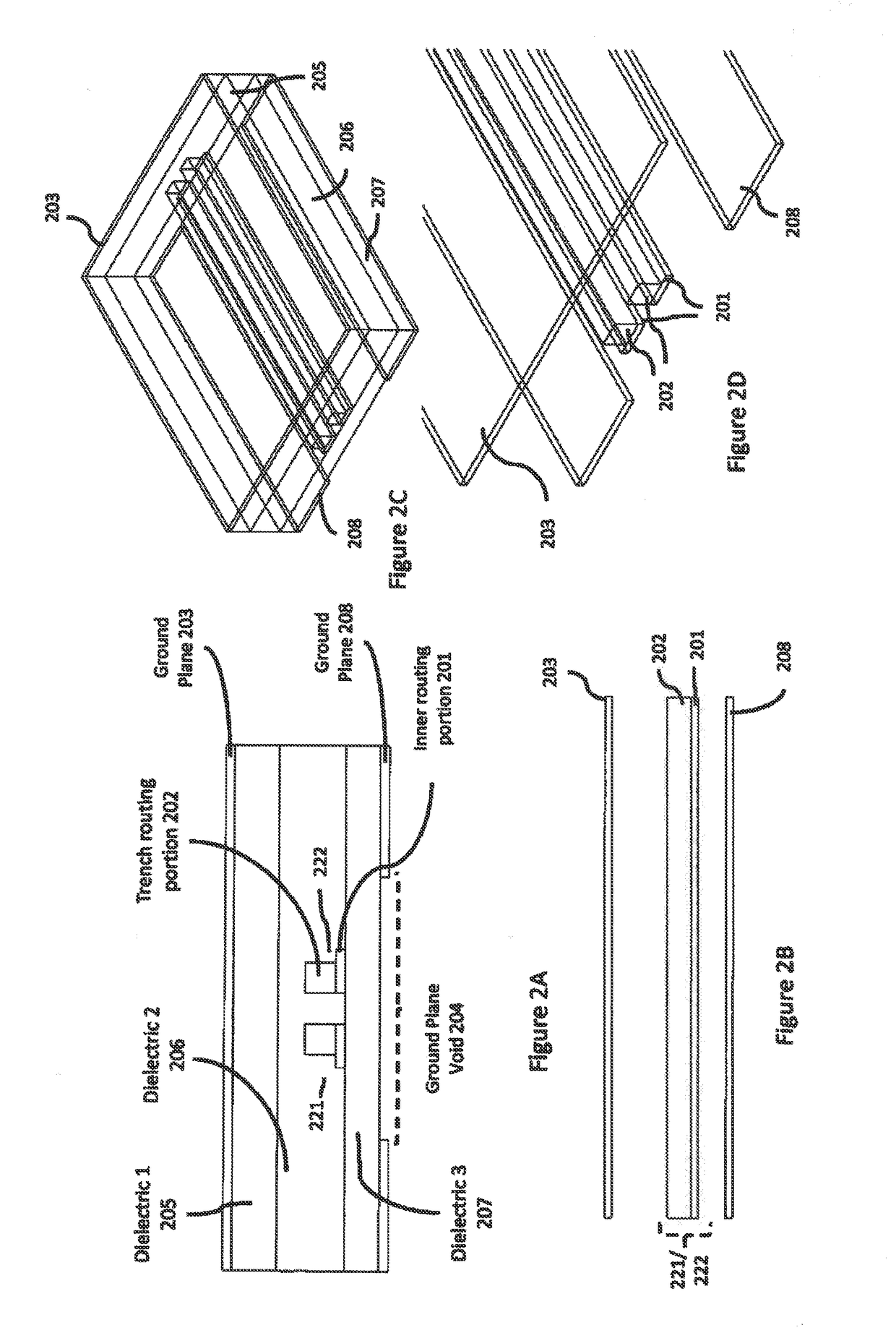
[0023]A substrate routing scheme that includes the use of trench routing is disclosed. In one embodiment, the substrate is a printed circuit board (PCB). Trench routing is used for signal conductors in a substrate. In one embodiment, the signal conductors are differential signal pairs (D+ and D−). The vertical trench can be designed at the outer or at inner sidewalls of D+ and D− differential signals.

[0024]FIGS. 1A-D illustrate one embodiment of bottom trench routing. FIG. 1A illustrates a cross section view of the bottom trench routing. Referring to FIG. 1A, two si...


PUM


Abstract

An interconnect topology that includes vertical trench routing in a substrate is disclosed. In one embodiment, the interconnect comprises a substrate having a plurality of layers including a first ground plane layer; a pair of signal conductors that form a differential signal pair, each conductor of the pair of signal conductors having a first portion and a second portion, the second portion extending from the first portion into at least one of the plurality of layers, wherein width of the second portion is less than width of the first portion; and wherein the first ground plane layer is only a first partial layer and has a first void region that is closer to the pair of signal conductors than the first partial layer.

Description

FIELD OF THE INVENTION[0001]Embodiments of the present invention relate to the field of substrate (e.g., printed circuit board (PCB)) routing; more particularly, embodiments of the present invention relate to substrates that include differential signal pairs in which each conductor includes a trench routing portion that extends from another routing portion.BACKGROUND OF THE INVENTION[0002]Conventional PCB routing configurations have channel length limitations when used in high speed signaling situations. When conventional routing configurations employ microstrip, stripline or dual stripline for high speed signaling, the platform channel length is usually limited to 7″ or less. For example, the Universal Serial Bus (USB) 3.1 channel length based on a dual-stripline in today's Ultrabook™ stack-up is limited to 6″ or 7″. A channel length larger than this will experience too much PCB loss or require circuit design capability or a costly on-board retimer, both of which increase the bill ...

Claims


Application Information

Patent Timeline
Patent Type & Authority Patents(United States)
IPC IPC(8): H05K7/00H01L21/48H01L23/00H01L23/498H01P3/00H01P3/02H01P3/04H01P3/08H01P5/02H05K1/00H05K1/02H05K1/11
CPCH01L21/4846H01L21/4857H01L21/486H01L23/49822H01L23/49827H01L24/10H01P3/082H05K1/0224H05K1/0245H05K2201/0376H05K3/462H05K3/4638H05K2201/098H05K2203/1189H05K1/0242H01P3/08H01P3/003H01P3/026H01P5/028H01P3/04
Inventor KONG, JACKSONCHEAH, BOK ENGYONG, KHANG CHOONGHECK, HOWARD L.CHEN, KUAN-YU
Owner INTEL CORP
Why Eureka
Try Eureka