Differential interconnect topology in a substrate with staggered vias

a topology and substrate technology, applied in the field of interconnect topologies, can solve the problems of large return loss and undesirable resonance behavior, hard to compensate or cancel out reflections due to via stubs, and completely impair links without proper mitigation

Inactive Publication Date: 2016-06-16
INTEL CORP
View PDF3 Cites 5 Cited by
  • Summary
  • Abstract
  • Description
  • Claims
  • Application Information

AI Technical Summary

Problems solved by technology

A long via stub on PCB platforms is usually capacitive in nature and causes large return loss and undesirable resonance behavior.
While compensation for PCB conductor and dielectric loss can be made with equalization circuits and PCB crosstalk can be addressed with stripline interconnections, reflections due to via stubs are hard to compensate for or cancel out, even using a limited tap decision feedback equalizer (DFE).
This phenomenon becomes more prominent if lower loss PCB materials are used and the data rate goes higher, in which case long via stubs can completely impair a link without proper mitigation.
Due to layout space constraints and discrete components (e.g., alterna

Method used


Image

  • Differential interconnect topology in a substrate with staggered vias
  • Differential interconnect topology in a substrate with staggered vias
  • Differential interconnect topology in a substrate with staggered vias

Examples


Embodiment Construction

[0015]The following description and the drawings sufficiently illustrate specific embodiments to enable those skilled in the art to practice them. Other embodiments may incorporate structural, logical, electrical, process, and other changes. Portions and features of some embodiments may be included in, or substituted for, those of other embodiments. Embodiments set forth in the claims encompass all available equivalents of those claims.

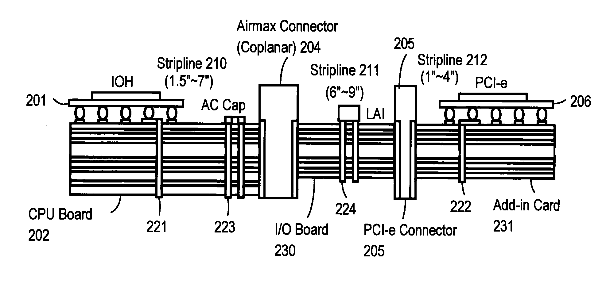
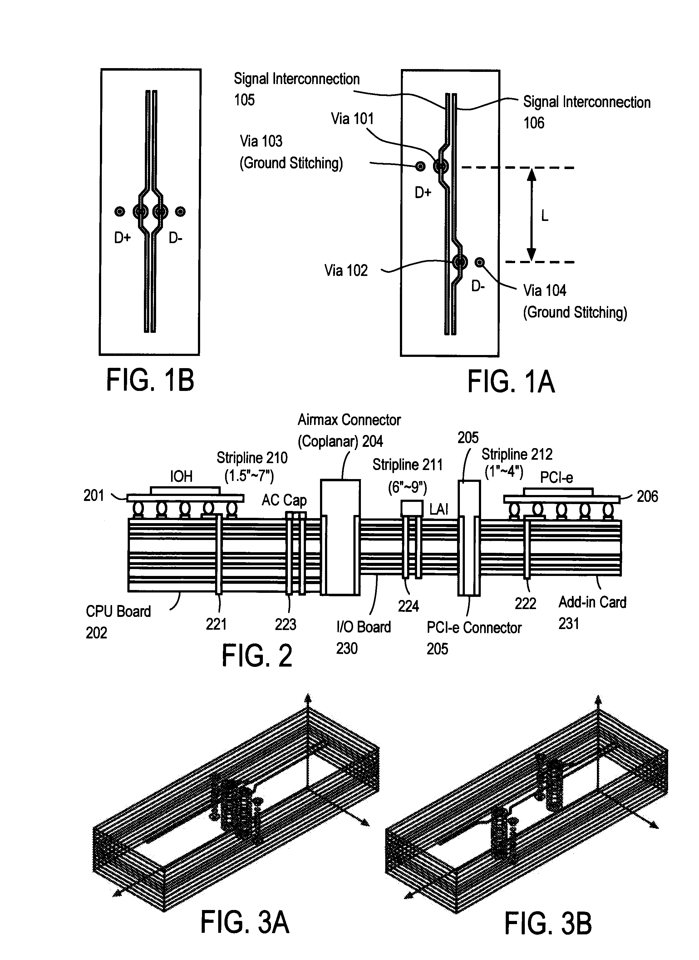
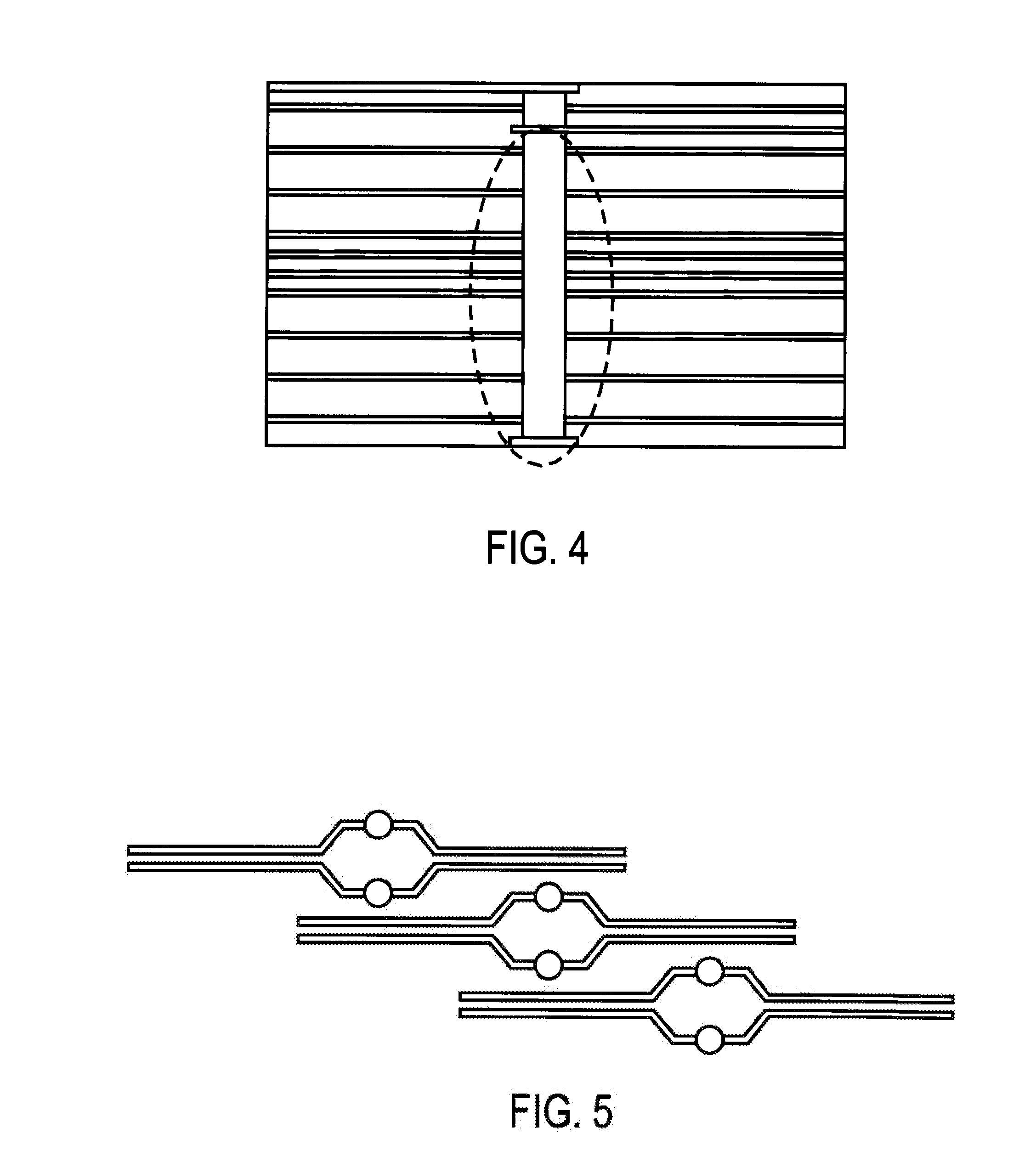
[0016]In one embodiment, the positive via and the negative via within a differential pair are routed in a staggered or skewed fashion in a substrate (e.g., printed circuit board (PCB). This is done in order to spread out the discontinuity or reflections from the positive interconnect and negative interconnect, thereby reducing the overall impedance discontinuity and improve the interconnect performance and / or bandwidth.

[0017]FIG. 1A illustrates one embodiment of a pair of vias in a staggered or skewed arrangement. The pair of vias are the positive and...


PUM


Abstract

An interconnect topology is disclosed that includes a plurality of interconnections, each of which is coupled together using a via, where at least two of the vias are staggered with respect to each other. In one embodiment, the interconnect topology comprises a substrate, multiple signal traces routed through the substrate on multiple layers, and a plurality of vias, where each via couples a pair of the signal traces to form an interconnection between different ones of the multiple layers, and where a pair of vias comprise a first via to carry a positive differential signal via and a second via to carry a negative differential signal that are coupled to signal traces to form a differential signal pair. The differential first and second vias are staggered with respect to each other.

Description

FIELD OF THE INVENTION[0001]Embodiments of the present invention relate to the field of interconnect topologies that include differential signal pairs in a substrate; more particularly, embodiments of the present invention relate to staggering a pair of vias that are part of interconnections forming a pair of differential signals in a substrate.BACKGROUND OF THE INVENTION[0002]A printed circuit board (PCB) includes a number of signal traces on a number of different layers that can be interconnected to form an interconnect topology. The interconnection of signal traces between the layers is often made using metal deposited through vias in the PCB that connects the two signal traces together. The portion of a via that extends through the PCB beyond the portion that interconnects the layers to form a signal path is referred to as a via stub.[0003]A long via stub on PCB platforms is usually capacitive in nature and causes large return loss and undesirable resonance behavior. A long via ...

Claims


Application Information

Patent Timeline
IPC IPC(8): H01P3/08
CPCH01P3/081H05K1/0245H01P3/026H05K1/0251H05K1/116H05K2201/09636
Inventor WANG, MINSHRYOCK, RUSSELL N.
Owner INTEL CORP
Why Eureka
Try Eureka