Supercharge Your Innovation With Domain-Expert AI Agents!

Simultaneous write, read, and command-address-control calibration of an interface within a circuit

a command-address control and parallel write technology, applied in the field of memory system calibration, can solve the problems of affecting computer system performance, reliability, timing variation and timing skew from one system implementation to another, and time-consuming calibration

Inactive Publication Date: 2018-10-02
IBM CORP
View PDF29 Cites 0 Cited by
  • Summary
  • Abstract
  • Description
  • Claims
  • Application Information

AI Technical Summary

Benefits of technology

The patent describes a method for testing an electronic circuit to identify areas of delay and ensure they are functioning properly. The method involves performing multiple tests simultaneously, adjusting the timing for each test, and iterating until certain edges are detected. The computer system and computer program product contain the necessary instructions for performing this test. The technical effects of the patent are improved efficiency and accuracy in identifying areas of delay in electronic circuits.

Problems solved by technology

Timing variations, frequency, temperature, aging, and other conditions impact data transfer rates to and from memory or other storage, which impacts computer system performance, and reliability.
Given the high clock rates and fast edge speed used in many computer systems, timing variations and timing skews from one system implementation to another are challenging and time consuming to calibrate, especially for systems with larger amounts of memory and a greater overall width of the memory bus.

Method used


Image

  • Simultaneous write, read, and command-address-control calibration of an interface within a circuit
  • Simultaneous write, read, and command-address-control calibration of an interface within a circuit
  • Simultaneous write, read, and command-address-control calibration of an interface within a circuit

Examples


Embodiment Construction

[0026]In the following description, for the purposes of explanation, numerous specific details are set forth in order to provide a thorough understanding of the present invention. It will be apparent, however, to one skilled in the art that the present invention may be practiced without these specific details. In other instances, well-known structures and devices are shown in block diagram form in order to avoid unnecessarily obscuring the present invention.

[0027]In addition, in the following description, for purposes of explanation, numerous systems are described. It is important to note, and it will be apparent to one skilled in the art, that the present invention may execute in a variety of systems, including a variety of computer systems and electronic devices operating any number of different types of operating systems.

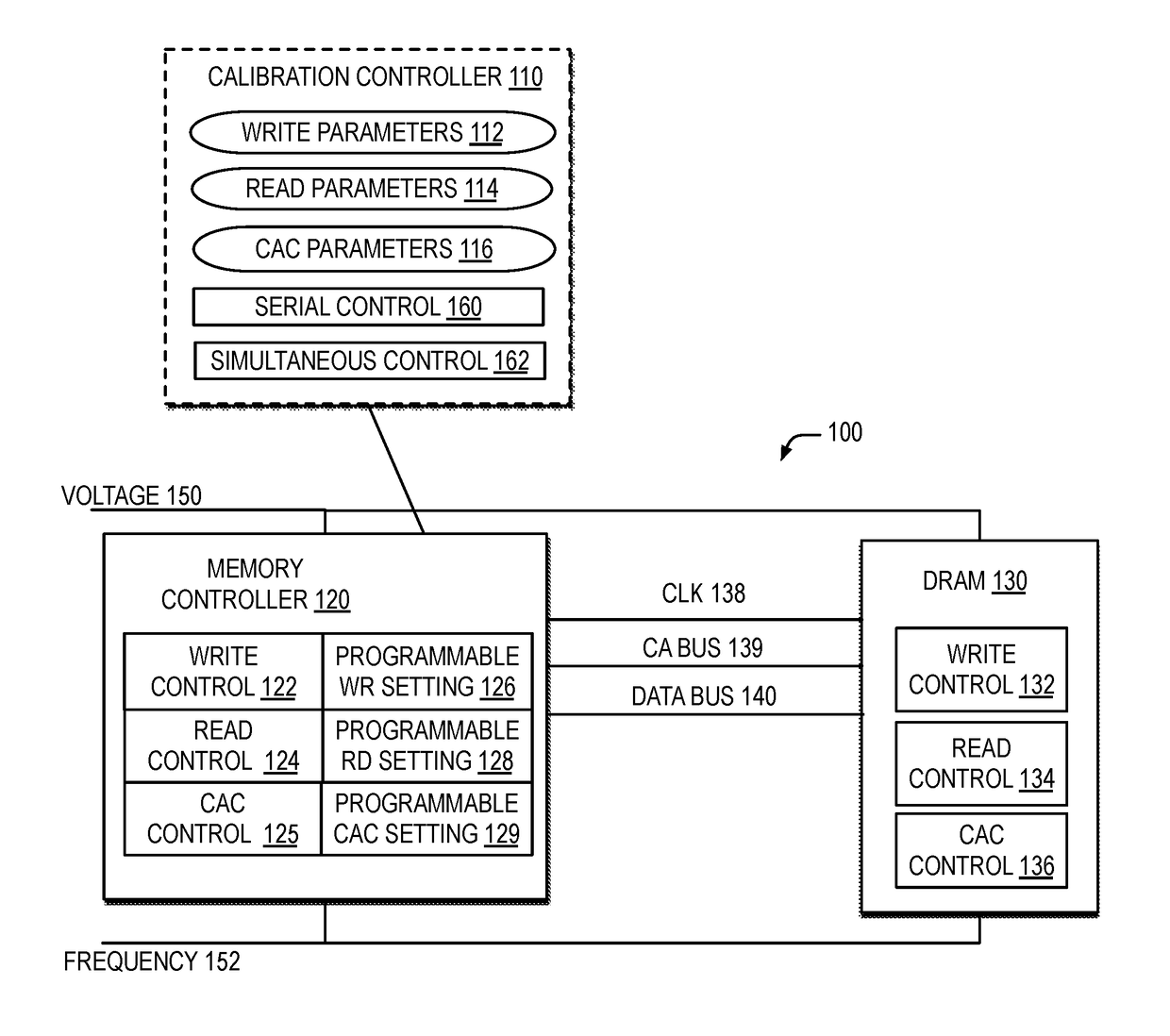
[0028]FIG. 1 illustrates a block diagram of one example of an electronic circuit including a calibration controller for managing simultaneous write, read, and CA...


PUM


Abstract

A calibration controller tests an electronic circuit to identify an initial read check with a read delay, an initial write check with a write delay, and an initial command, address, control (CAC) check with a CAC delay indicated as passing. Responsive to the initial read check, the initial write check, and the initial CAC check indicated as passing, for each setting of the read delay, the write delay, and the CAC delay, the calibration controller iteratively performs concurrently, a write test with the write delay, a read test with the read delay, and a CAC test with the CAC delay on the electronic circuit over the range of conditions while simultaneously adjusting the write delay, the read delay, and the CAC delay for each iteration until one or more of a read edge, a write edge, and a CAC edge are detected.

Description

BACKGROUND1. Technical Field[0001]This invention relates in general to a memory system calibration and more particularly to simultaneous write, read, and command-address-control (CAC) calibration of an interface within a circuit.2. Description of the Related Art[0002]Computing systems generally include one or more circuits with one or more memory or storage devices connected to one or more processors via one or more controllers. Timing variations, frequency, temperature, aging, and other conditions impact data transfer rates to and from memory or other storage, which impacts computer system performance, and reliability. As operating frequencies increase, the valid window for read signals, write signals, and CAC signals to be latched within decreases. Given the high clock rates and fast edge speed used in many computer systems, timing variations and timing skews from one system implementation to another are challenging and time consuming to calibrate, especially for systems with larg...

Claims


Application Information

Patent Timeline
Patent Type & Authority Patents(United States)
IPC IPC(8): G11C29/50G11C8/18G11C29/52G11C7/22
CPCG11C29/50012G11C29/52G11C8/18G11C7/22G11C29/023G11C29/028G11C2029/2602G11C7/109G11C11/4072G11C11/4076G11C2207/2254G11C7/00
Inventor GLANCY, STEPHEN P.NEATON, JEREMY R.VAN HUBEN, GARY A.
Owner IBM CORP
Features
  • R&D
  • Intellectual Property
  • Life Sciences
  • Materials
  • Tech Scout
  • Unparalleled Data Quality
  • Higher Quality Content
  • 60% Fewer Hallucinations
Learn More