Page access circuit of semiconductor memory device

a memory device and access circuit technology, applied in static storage, information storage, digital storage, etc., can solve the problems of short refresh cycle, low standby current condition required, and degraded processing system performan

Active Publication Date: 2006-11-23
SK HYNIX INC
View PDF10 Cites 30 Cited by
  • Summary
  • Abstract
  • Description
  • Claims
  • Application Information

AI Technical Summary

Benefits of technology

[0030] According to one embodiment of the present invention, a page access control circuit of a semiconductor memory device comprises an address transition detecting unit adapted and configured to generate a page address transition detecting signal, a column control unit controlled by a page address control signal, a column selecting unit adapted and configured to generate a column selecting signal in response to the write/read operation strobe signal, a page control unit controlled by a sense detecting signal which represents completion of an operation of a bit line sense amplifier, a pre-active unit, and a precharge unit controlled by the page address active precharge identification signal. The

Problems solved by technology

However, when the refresh cycle becomes short, an external processing device is inaccessible to the DRAM, so that the performance of the processing system is degraded.
Additionally, when the refresh cycle becomes short, current consumption for the refresh operation is increased.
Specifically, the

Method used


Image

  • Page access circuit of semiconductor memory device
  • Page access circuit of semiconductor memory device
  • Page access circuit of semiconductor memory device

Examples


Embodiment Construction

[0039] The present invention will be described in detail with reference to the accompanying drawings. Wherever possible, the same reference numbers will be used throughout the drawings to refer to the same or like parts.

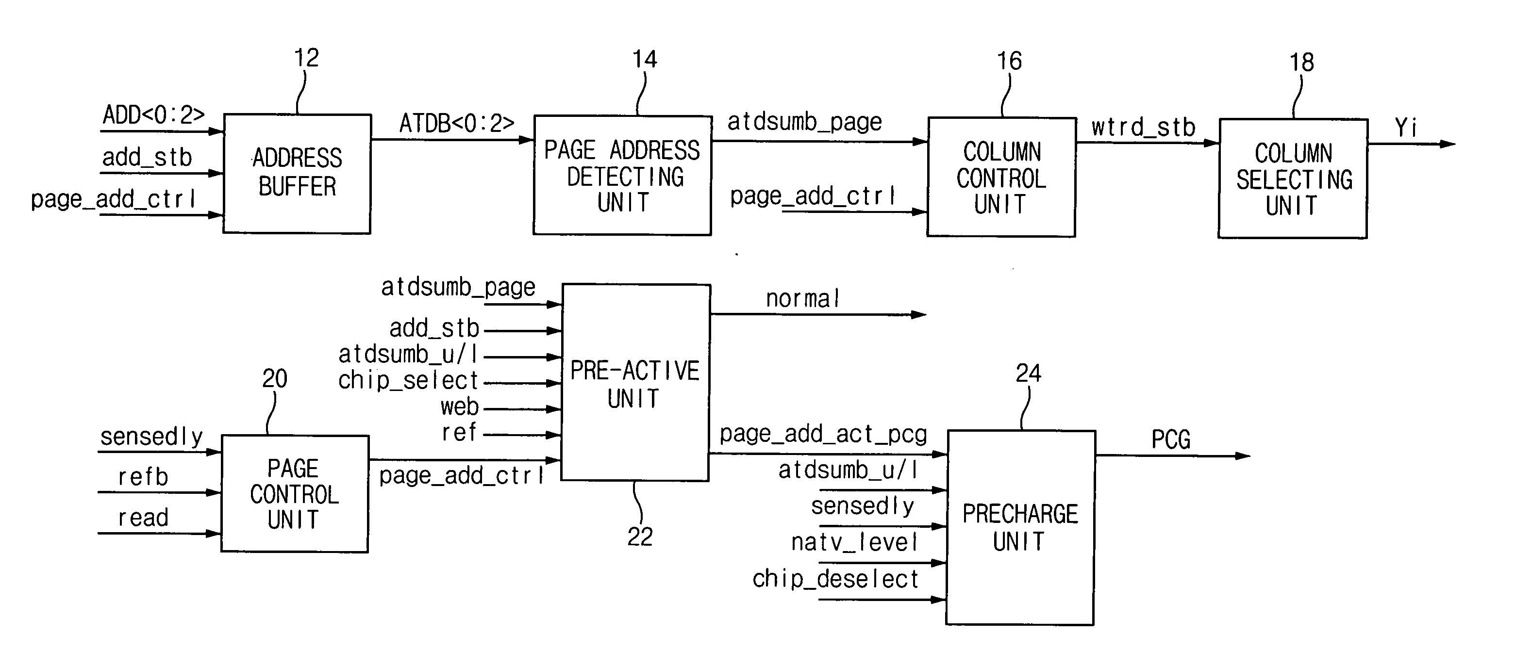
[0040]FIG. 3 is a block diagram illustrating a page access control circuit of a PSRAM according to an embodiment of the present invention.

[0041] In this embodiment, a page access control circuit comprises an address buffer 12, a page address detecting unit 14, a column control unit 16, a column selecting unit 18, a page control unit 20, a pre-active unit 22 and a precharge unit 24.

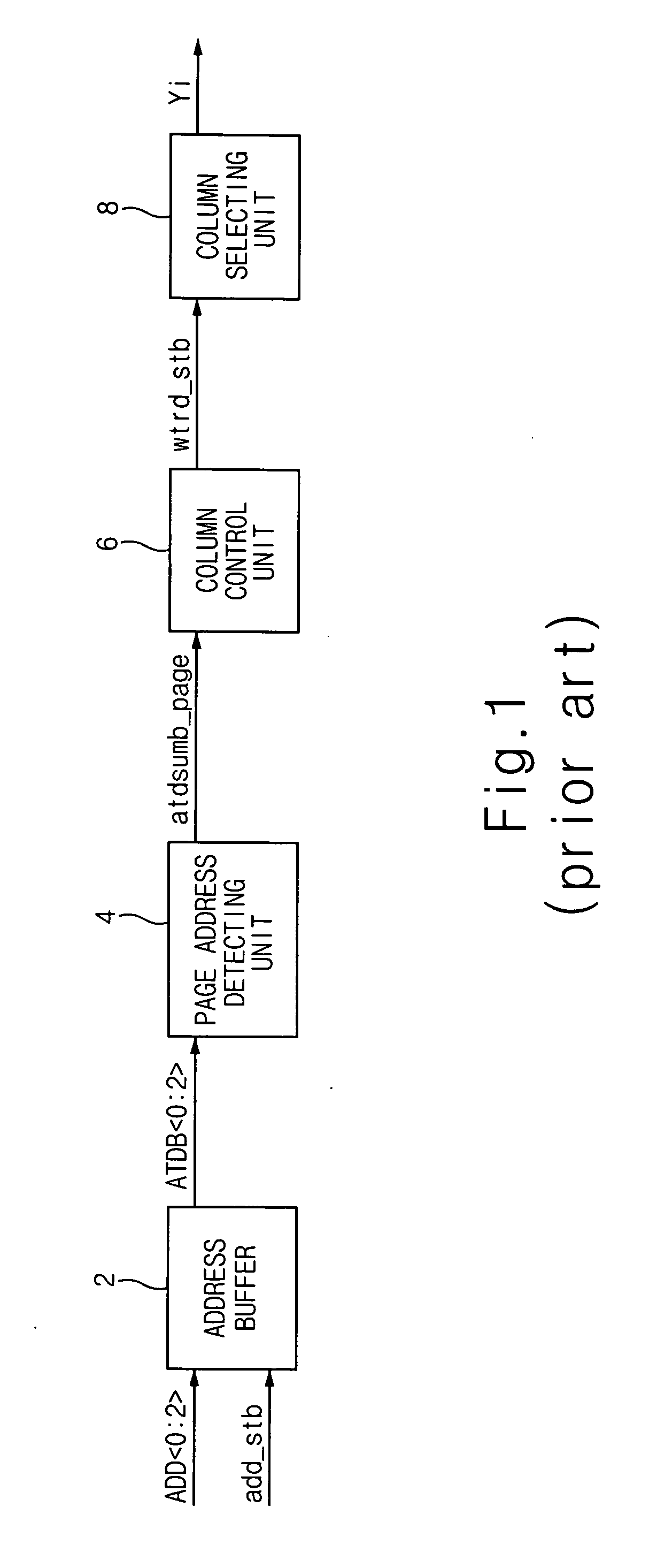
[0042] The address buffer 12 receives a page address ADD from an external address pin to detect a transition timing of the page address ADD in response to an address strobe signal add_stb and a page address control signal page_add_ctrl, thereby generating address transition detecting signals ATDB21 0:2>.

[0043] The page address detecting unit 14 generates a page address detecting signal ...


PUM


Abstract

Abstract of the Disclosure A page access circuit of a semiconductor memory device is normally operated even when a page address toggles at any timing in a page mode. The page access circuit comprises an address buffer, a column control unit, a page control unit, a pre-active unit and a precharge unit. The column control unit is controlled by the page address control signal. The page control unit controlled by a sense detecting signal is adapted and configured to generate the page address control signal. The pre-active unit controlled by the page address control signal is adapted and configured to generate a mode identification signal in response to the page address transition detecting signal. The precharge unit is adapted and configured to perform a selective precharge operation in response to the mode identification signal.

Description

BACKGROUND OF THE INVENTION [0001] 1. Field of the Invention [0002] The present invention generally relates to an active control circuit of a Pseudo Static Random Access Memory (hereinafter, referred to as “PSRAM”), and more specifically, to a technology of enabling a normal operation even when a page address toggles at any timing in a page operation. [0003] 2. Description of the Related Art [0004] In general, a Dynamic Random Access Memory (hereinafter, referred to as “DRAM”) memorizes information as a type of charges in a capacitor, shares the charges in a corresponding bit line through a transistor, and amplify the shared charges in a sense amplifier to read data. [0005] The above-described DRAM which comprises a transistor and a capacitor embodies a memory having a large memory capacity with a small area. [0006] Meanwhile, elements of a memory device become miniaturized for the purpose of high-speed operation of memory devices, reduction of current consumption and miniaturizatio...

Claims


Application Information

Patent Timeline
IPC IPC(8): G11C7/00
CPCG11C7/1021G11C11/34G11C11/415
Inventor LEE, YIN JAE
Owner SK HYNIX INC
Why Eureka
Try Eureka