Supercharge Your Innovation With Domain-Expert AI Agents!

Multiple mode device implementation for programmable logic devices

a logic device and multi-mode technology, applied in the direction of generating/distributing signals, pulse techniques, instruments, etc., can solve the problems of occupying the most of the timing budget associated with a particular user design, restricting plb utilization, and consuming most of the available power

Active Publication Date: 2018-11-27
LATTICE SEMICON CORP
View PDF15 Cites 0 Cited by
  • Summary
  • Abstract
  • Description
  • Claims
  • Application Information

AI Technical Summary

Benefits of technology

The patent text describes techniques for improving the efficiency of implementing user designs in programmable logic devices (PLDs) by increasing the flexibility of logic cells and routing resources. This allows for additional degrees of freedom in the routing when implementing a particular user design, resulting in improved utilization of the PLD's resources. The text also discusses the role of routing structures in PLDs and how they impact the area, power, and delay of the fabric. Overall, the patent text provides a solution for maximizing functionality while minimizing the area, power, and delay of PLDs.

Problems solved by technology

The routing resources flexibly connect the logic blocks and / or cells to one another and can constitute greater than 65% of the area of the PLD, can consume most of the available power, and can take up most of a timing budget associated with a particular user design.
As such, routing limitations restrict PLB utilization.
PLB utilization can be improved by increasing the amount of available routing resources, but such increases consume more area.

Method used


Image

  • Multiple mode device implementation for programmable logic devices
  • Multiple mode device implementation for programmable logic devices
  • Multiple mode device implementation for programmable logic devices

Examples


Embodiment Construction

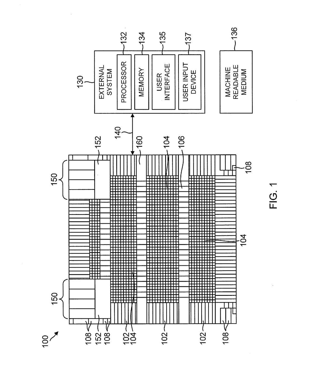
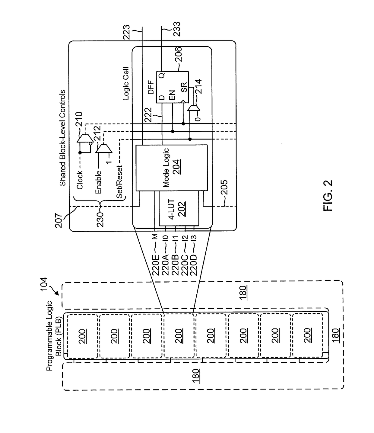
[0014]In accordance with embodiments set forth herein, techniques are provided to efficiently implement user designs in programmable logic devices (PLDs). In various embodiments, a user design may be converted into and / or represented by a set of PLD components (e.g., configured for logic, arithmetic, or other hardware functions) and their associated interconnections available in a PLD. For example, a PLD may include a number of programmable logic blocks (PLBs), each PLB including a number of logic cells, and configurable routing resources that may be used to interconnect the PLBs and / or logic cells. In some embodiments, each PLB may be implemented with between 2 and 16 or between 2 and 32 logic cells.

[0015]In various embodiments, PLB utilization in a PLD can be improved by increasing the flexibility of the PLBs, logic cells, and / or routing resources to allow for additional degrees of freedom in the routing when implementing a particular user design. Such additional degrees of freedo...


PUM


Abstract

Various techniques are provided to efficiently implement user designs in programmable logic devices (PLDs). In one example, a programmable logic device (PLD) includes a plurality of programmable logic blocks (PLBs) and at least first and second logic cells within at least one of the PLBs, where each logic cell includes a lookup table (LUT) and associated mode logic configured to receive a LUT output signal from the LUT. The associated mode logic is configured to use a single physical signal output to provide a logic cell output signal corresponding to a selected logic function operational mode, ripple arithmetic operational mode, or extended logic function operational mode for each logic cell.

Description

CROSS-REFERENCE TO RELATED APPLICATIONS[0001]This patent application is a continuation of U.S. patent application Ser. No. 14 / 610,127 filed Jan. 30, 2015, which claims priority to and the benefit of U.S. Provisional Patent Application 62 / 028,441 filed Jul. 24, 2014, all of which are hereby incorporated by reference in their entirety.TECHNICAL FIELD[0002]The present invention relates generally to programmable logic devices and, more particularly, to gate-level arrangements implemented in such devices.BACKGROUND[0003]Programmable logic devices (PLDs) (e.g., field programmable gate arrays (FPGAs), complex programmable logic devices (CPLDs), field programmable systems on a chip (FPSCs), or other types of programmable devices) may be configured with various user designs to implement desired functionality. Typically, the user designs are synthesized and mapped into configurable resources (e.g., programmable logic gates, look-up tables (LUTs), embedded hardware, or other types of resources...

Claims


Application Information

Patent Timeline
Patent Type & Authority Patents(United States)
IPC IPC(8): H03K19/173H03K19/00H03K3/356H03K19/177G06F17/50H03K3/3562
CPCH03K3/35625G06F17/505G06F17/5054H03K19/17728H03K19/0016H03K19/173H03K3/356156G06F1/10G06F1/3275G06F30/34G06F30/327G06F30/347
Inventor SHARPE-GEISLER, BRADGUNARATNA, SENANIYEW, TING
Owner LATTICE SEMICON CORP
Features
  • R&D
  • Intellectual Property
  • Life Sciences
  • Materials
  • Tech Scout
  • Unparalleled Data Quality
  • Higher Quality Content
  • 60% Fewer Hallucinations
Learn More