OLED panel manufacturing method and OLED panel

a manufacturing method and technology of oled panels, applied in the field of display, can solve the problems of difficult printing process to manufacture high-resolution (e.g., 4k) oled panels, and achieve the effects of reducing lateral leakage, increasing oled panel resolution, and reducing lateral leakag

Active Publication Date: 2018-12-25
SHENZHEN CHINA STAR OPTOELECTRONICS SEMICON DISPLAY TECH CO LTD
View PDF7 Cites 0 Cited by
  • Summary
  • Abstract
  • Description
  • Claims
  • Application Information

AI Technical Summary

Benefits of technology

[0005]The object of the present invention is to provide an OLED panel manufacturing method, able to increase OLED panel resolution without changing printing accuracy to achieve stable, reliable isolation and insulation between pixel electrodes.
[0006]Another object of the present invention is to provide an OLED, panel, with higher resolution as well as stable, reliable isolation and insulation between pixel electrodes.
[0034]Compared to the known techniques, the present invention provides the following advantages: the present invention provides an OLED panel manufacturing method, forming a first pixel electrode inside each pixel unit and a second pixel electrode separated from the first pixel electrode; depositing an insulation film by an atomic layer deposition method, and patternizing to form a pixel electrode isolation insulation layer; the pixel electrode isolation insulation layer having a longitudinal portion filling between the first and second pixel electrodes, and a latitudinal portion having both ends covering respectively a part of the first pixel electrode closer to the second pixel electrode and a part of the second pixel electrode closer to the first pixel electrode; forming a pixel isolation layer, and printing LOED elements; the present invention can increase OLED panel resolution without changing printing accuracy so that the first and second pixel electrodes are completely insulated, to achieve reducing lateral leakage between the first and second pixel electrodes. The present invention provides an OLED panel, each pixel unit disposed with a first pixel electrode, a second pixel electrode, a pixel electrode isolation insulation layer for isolating and insulating the first and second pixel electrodes, and an OLED light-emitting device deposited on the first pixel electrode, second pixel electrode, and the pixel electrode isolation insulation layer; the pixel electrode isolation insulation layer can assure complete insulation between the first and second pixel electrodes and reduce lateral leakage between the first and second pixel electrodes.

Problems solved by technology

However, due to the printing contemporary printing capability limitation, it is difficult to use a printing process to manufacture a high-resolution (e.g., 4K) OLED panel.
The main reason is that the contemporary printing technology is unable to perfectly print an OLED light-emitting device 202 in a very small pixel unit, due to ink overflow, and resulting in color mixing.

Method used


Image

  • OLED panel manufacturing method and OLED panel
  • OLED panel manufacturing method and OLED panel
  • OLED panel manufacturing method and OLED panel

Examples


Embodiment Construction

[0041]To further explain the technical means and effect of the present invention, the following refers to embodiments and drawings for detailed description.

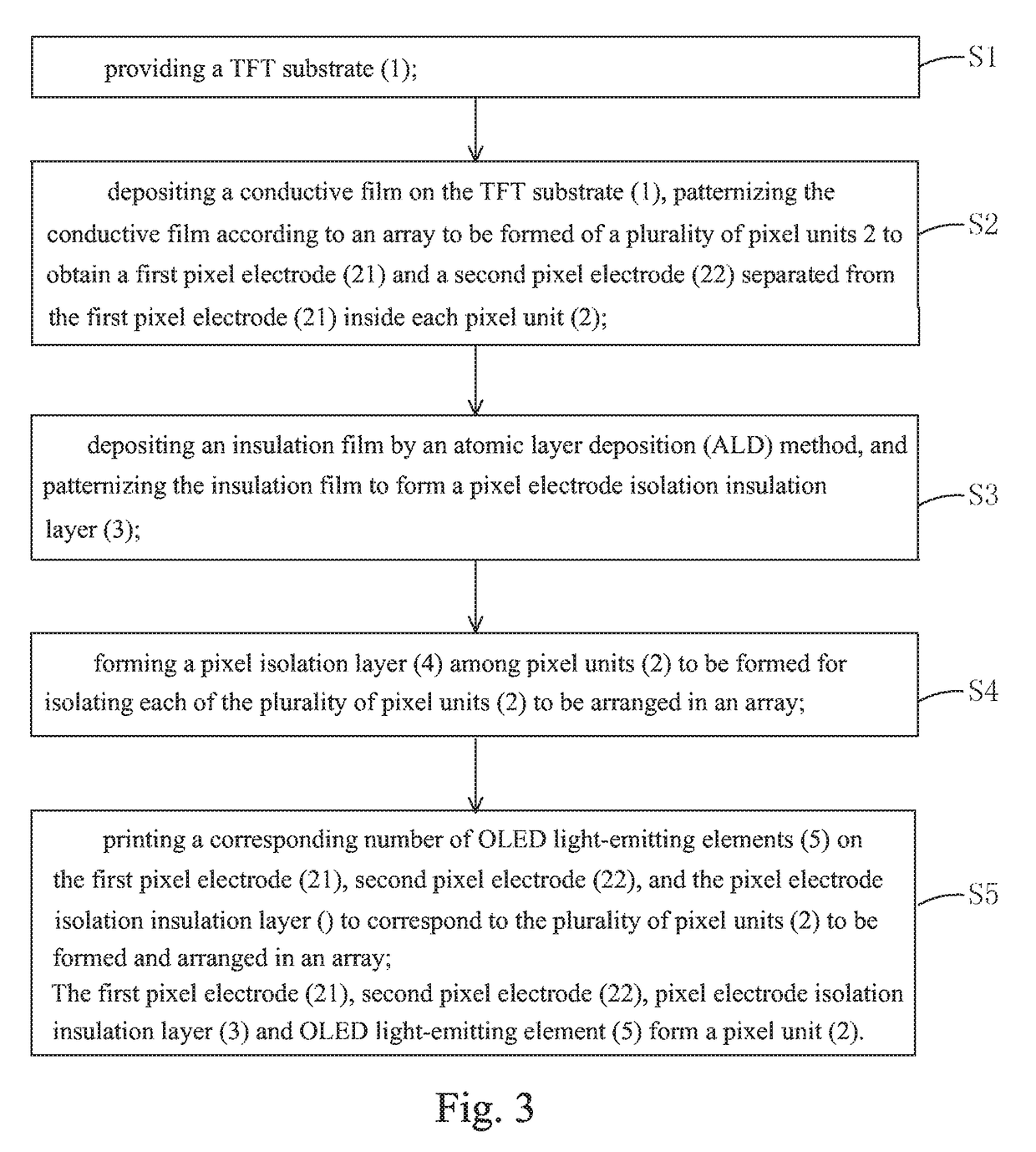
[0042]Refer to FIG. 3, in combination with FIGS. 4 and FIG. 5. The present invention provides an organic light-emitting diode (OLED) manufacturing method, comprising the steps of:

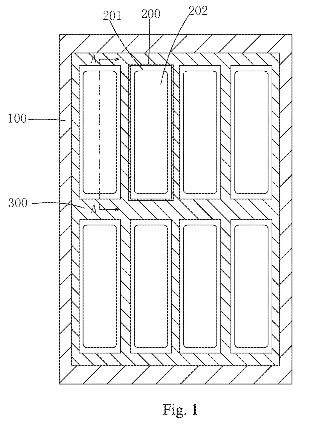
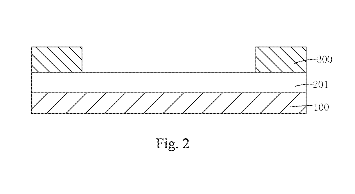
[0043]Step S1: providing a thin film transistor (TFT) substrate 1.

[0044]Specifically, the TFT substrate 1 has a thickness of 500 Å to 1000 Å, which usually comprises a glass base, gates, scan lines, gate insulation layer, active layer, interlayer insulation layer, sources, drains, data lines, and so on, and is the same as the prior art; thus, the detailed description will be omitted.

[0045]Step S2: depositing a conductive film on the TFT substrate 1, patternizing the conductive film according to an array to be formed of a plurality of pixel units 2 to obtain a first pixel electrode 21 inside each pixel unit 2 and a second pixel electrode 22 separated from...


PUM


Abstract

The invention provides an OLED panel manufacturing method and OLED panel. The method comprises: forming first (21) and second (22) pixel electrodes inside each pixel unit (2); depositing an insulation film by an atomic layer deposition method, and patternizing to form a pixel electrode isolation insulation layer (3); the pixel electrode isolation insulation layer having a longitudinal portion (31) filling between the first (21) and second (22) pixel electrodes, and a latitudinal portion (32) having both ends covering respectively a part of the first pixel electrode (21) closer to the second pixel electrode (22) and a part of the second pixel electrode (22) closer to the first pixel electrode (21); forming a pixel isolation layer (4), and printing LOED elements (5); the invention can increase OLED panel resolution without changing printing accuracy so that the first (21) and second (22) pixel electrodes are completely insulated.

Description

BACKGROUND OF THE INVENTION1. Field of the Invention[0001]The present invention relates to the field of display, and in particular to an organic light-emitting diode (OLED) panel manufacturing method and OLED panel.2. The Related Arts[0002]The organic light-emitting diode (OLED) panel has the advantages of active light-emitting, low driving voltage, high emission efficiency, quick response time, high resolution and contrast, near 180° viewing angle, wide operation temperature range, and capability to realize flexible display and large-area full-color display, and is regarded as the most promising display technology.[0003]Refer to FIG. 1 and FIG. 2. A conventional OLED panel comprises: a thin film transistor (TFT) substrate 100, a plurality of pixel units 200 arranged in an array on the TFT substrate 100, a pixel isolation layer 300 filling between adjacent pixel units 200 in the array of the plurality of pixel units to isolate each pixel unit 200 from adjacent pixel units 20, wherei...

Claims


Application Information

Patent Timeline
Patent Type & Authority Patents(United States)
IPC IPC(8): H01L21/00H01L51/00H01L27/32H01L51/56
CPCH01L27/3246H01L51/56H01L51/0004H01L2227/323H10K59/122H10K71/13H10K59/1201H10K71/00H10K71/20
Inventor ZHANG, XIAOXING
Owner SHENZHEN CHINA STAR OPTOELECTRONICS SEMICON DISPLAY TECH CO LTD
Why Eureka
Try Eureka