Hermetic sealing cap, electronic component housing package, and method for manufacturing hermetic sealing cap

a technology of electronic components and sealing caps, which is applied in the direction of hermetically sealed casings, manufacturing tools, basic electric elements, etc., can solve the problems of reduced solder in the sealing region and insufficient sealing, and achieve the effect of suppressing the reduction of solder

Active Publication Date: 2019-01-22
HITACHI METALS LTD
View PDF11 Cites 1 Cited by
  • Summary
  • Abstract
  • Description
  • Claims
  • Application Information

AI Technical Summary

Benefits of technology

[0007]The present invention has been proposed in order to solve the aforementioned problem, and an object of the present invention is to provide a hermetic sealing cap capable of suppressing a reduction in the amount of solder in a region bonded with an electronic component housing member by suppressing spread of part of melted solder to the outer surface of the hermetic sealing cap, an electronic component housing package employing the hermitic sealing cap, and a method for manufacturing the hermetic sealing cap.
[0026]According to the present invention, as hereinabove described, the first plated layer is exposed to be oxidized in the fourth region adjacent to the first region outside the first region, whereby the wettability to solder can be reduced in the fourth region outside the first region, and hence spread of the solder can be suppressed. Thus, part of melted solder can be inhibited from reaching the outer surface of the hermetic sealing cap. Consequently, spread of the part of the melted solder to the outer surface of the hermetic sealing cap can be suppressed when the hermetic sealing cap is bonded to the electronic component housing member, and hence a reduction in the amount of the solder in a region bonded with the electronic component housing member can be suppressed. Thus, the sealability of the electronic component housing package can be sufficiently ensured.
[0027]Furthermore, a region inside the first region is sectioned into the second region not adjacent to the first region and the third region adjacent to the first region, and the first plated layer is exposed to be oxidized in the third region. Thus, the wettability to solder can be reduced also in the third region inside the first region, and hence spread of the solder can be suppressed. Thus, the reduction in the amount of the solder in the region bonded with the electronic component housing member can be suppressed. In addition, the second plated layer of the second region not adjacent to the first region is left, whereby the appearance of a defect on a surface of the hermetic sealing cap can be suppressed by covering the first plated layer with the second plated layer in the second region not adjacent to the first region even in the case where there is a defect such as a pinhole in the first plated layer of the second region. Thus, the corrosion resistance can be improved in the second region not adjacent to the first region (inside the third region) while the spread of the solder is suppressed in the third region adjacent to the first region inside the first region bonded with the electronic component housing member through the solder.
[0028]Furthermore, in the aforementioned method for manufacturing a hermetic sealing cap according to the third aspect, the second plated layer of the third region adjacent to the first region and the second plated layer of the fourth region outside the first region are removed by the laser, whereby the second plated layer of the third region and the second plated layer of the fourth region can be easily removed without forming masks or the like on portions where the second plated layer is not removed, and corrosion of the first plated layer and the second plated layer caused by a reagent employed to remove the masks can be suppressed. Furthermore, the surface of the first plated layer of the third region and the fourth region is exposed by the laser, and the exposed surface of the first plated layer is oxidized, whereby no step of oxidizing the surface of the first plated layer exposed separately may be required, and hence the manufacturing process can be simplified.

Problems solved by technology

In this case, the amount of solder in the sealing region is reduced, and hence the sealability is not sufficiently ensured.

Method used


Image

  • Hermetic sealing cap, electronic component housing package, and method for manufacturing hermetic sealing cap
  • Hermetic sealing cap, electronic component housing package, and method for manufacturing hermetic sealing cap
  • Hermetic sealing cap, electronic component housing package, and method for manufacturing hermetic sealing cap

Examples


first embodiment

[0040](First Embodiment)

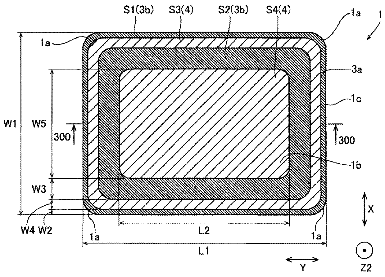
[0041]The structure of an electronic component housing package 100 according to a first embodiment of the present invention is now described with reference to FIGS. 1 to 4.

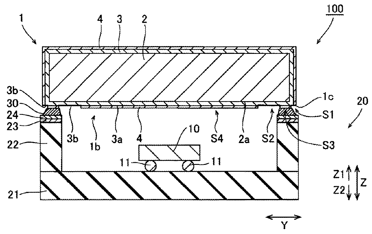
[0042]The electronic component housing package 100 according to the first embodiment of the present invention includes a hermetic sealing cap 1, an electronic component 10 such as a crystal oscillator, and an electronic component housing member 20 for housing the electronic component 10, as shown in FIG. 1.

[0043]The electronic component housing member 20 includes a ceramic substrate 21 and a ceramic frame body 22 each made of an insulating material such as alumina. The ceramic substrate 21 is a plate-like member, and the ceramic frame body 22 is arranged along the outer periphery on the upper surface of the ceramic substrate 21 and extends upward (Z1 side) at a prescribed height. The electronic component 10 is mounted through bumps 11 on the ceramic substrate 21 in a housing space surrounde...

second embodiment

[0072](Second Embodiment)

[0073]A second embodiment is now described with reference to FIGS. 8 and 9. According to this second embodiment, in addition to the aforementioned structure according to the first embodiment, protrusion regions S2b are provided in regions corresponding to corners 1a in an oxidized region S2a of a hermetic sealing cap 201.

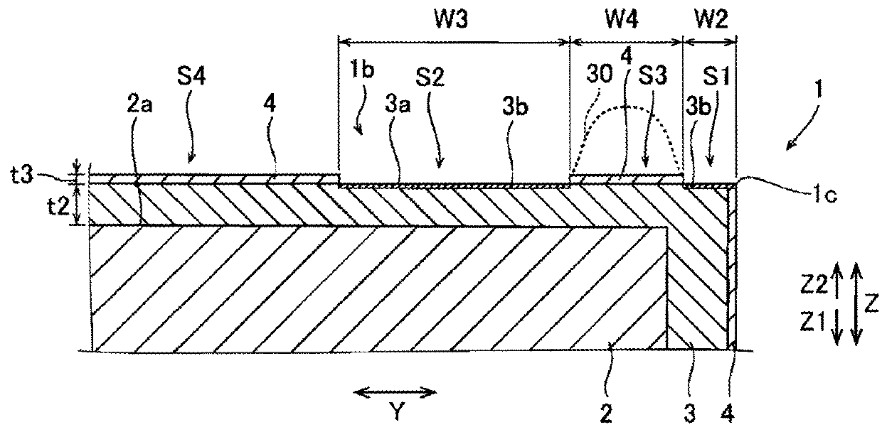
[0074]The hermetic sealing cap 201 according to the second embodiment of the present invention is sectioned into four regions of an oxidized region S1, the oxidized region S2a, a solder region S3a, and a plated region S4, as shown in FIG. 8. In the oxidized region S2a, a Au plated layer 4 is removed to expose a surface 3a of a Ni plated layer 3, and the exposed surface 3a of the Ni plated layer 3 is oxidized to form an oxide film layer 3b. The oxidized region S2a and the solder region S3a are examples of the “third region” and the “first region” in the present invention, respectively.

[0075]According to the second embodiment, the protrusion r...


PUM

PropertyMeasurementUnit
thickness t1aaaaaaaaaa
length L1aaaaaaaaaa
width W1aaaaaaaaaa

Abstract

A hermetic sealing cap includes a base material, a first plated layer formed on the base material, and a second plated layer formed on the first plated layer. A surface of the base material is sectioned into a first region, a second region not adjacent to the first region inside the first region, a third region adjacent to the first region inside the first region, and a fourth region adjacent to the first region outside the first region. In the third region and the fourth region, the first plated layer is exposed to be oxidized.

Description

BACKGROUND OF THE INVENTION[0001]Field of the Invention[0002]The present invention relates to a hermetic sealing cap, an electronic component housing package, and a method for manufacturing a hermetic sealing cap, and more particularly, it relates to a hermetic sealing cap bonded with an electronic component housing member through solder, an electronic component housing package employing the hermetic sealing cap, and a method for manufacturing the hermetic sealing cap.[0003]Description of the Background Art[0004]A hermetic sealing cap bonded with an electronic component housing member through solder is known in general, as disclosed in Japanese Patent Laying-Open No. 4-096256 (1992), for example.[0005]FIG. 5 of the aforementioned Japanese Patent Laying-Open No. 4-096256 discloses a metal hermetic sealing cap made of a material obtained by cladding Alloy 42(42 Ni—Fe alloy) and nickel, bonded to a package. In an entire region inside a ring-shaped sealing region formed at and near an o...

Claims


Application Information

Patent Timeline
Patent Type & Authority Patents(United States)
IPC IPC(8): H05K5/06B23K31/02H01L23/10
CPCB23K31/02H01L23/10H01L2224/16225H01L2924/0002H01L2924/00
Inventor NAGATOMO, KAZUYAASADA, KEN
Owner HITACHI METALS LTD
Why Eureka
Try Eureka