Low cost metallization during fabrication of an integrated circuit (IC)
- Summary
- Abstract
- Description
- Claims
- Application Information
AI Technical Summary
Benefits of technology
Problems solved by technology
Method used
Image

Examples
Embodiment Construction
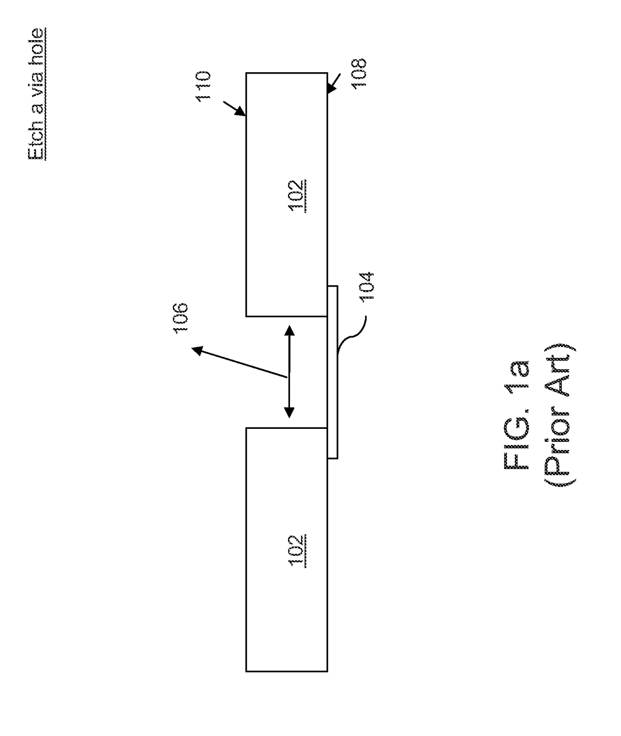
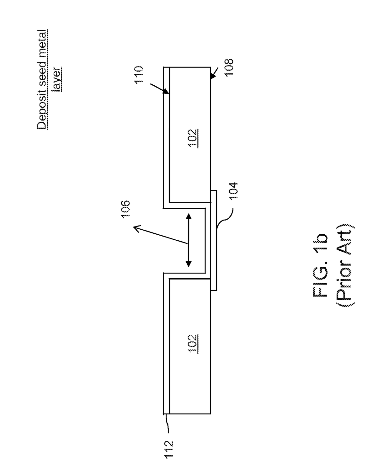
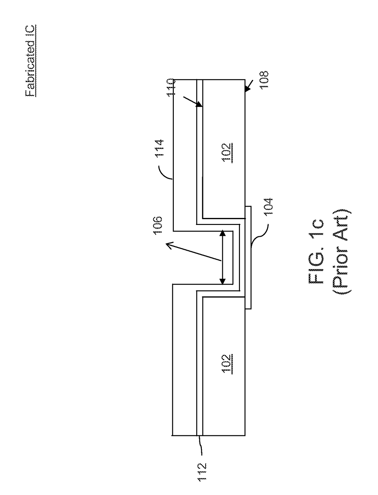
[0016]The detailed description of the appended drawings is intended as a description of the currently preferred embodiments of the present invention, and is not intended to represent the only form in which the present invention may be practiced. It is to be understood that the same or equivalent functions may be accomplished by different embodiments that are intended to be encompassed within the spirit and scope of the present invention.
[0017]The present invention proposes an improved method for metallization during a fabrication process of an IC. In particular, the present invention discloses a method for metalizing only the via holes on the semiconductor wafer, thereby saving a huge amount of metal that was being used during the metallization process in the conventional solutions.
[0018]FIG. 2a, FIG. 2b, FIG. 2c, FIG. 2d, FIG. 2e, FIG. 2f, and FIG. 2g are cross sectional diagrams of a semiconductor wafer 202, in accordance with an embodiment of the present invention.
[0019]FIG. 2a, ...
PUM
 Abstract
Description
Claims
Application Information
 - R&D Engineer
- R&D Manager
- IP Professional
- Industry Leading Data Capabilities
- Powerful AI technology
- Patent DNA Extraction
Browse by: Latest US Patents, China's latest patents, Technical Efficacy Thesaurus, Application Domain, Technology Topic.
© 2024 PatSnap. All rights reserved.Legal|Privacy policy|Modern Slavery Act Transparency Statement|Sitemap