

Antenna and electronic device including the same
a technology of electronic devices and antennas, applied in the field of electronic devices, can solve the problems of limited antenna volume space, difficult to implement all bands in a single antenna, spatial limit to changing the ground position to cover the shift of various operating frequencies of the low band, etc., to achieve the effect of preventing and/or reducing the degradation of the radiation performance of the antenna, and contributing to the slimness of the electronic devi
- Summary
- Abstract
- Description
- Claims
- Application Information
AI Technical Summary
Benefits of technology
Problems solved by technology
Method used
Image

Examples
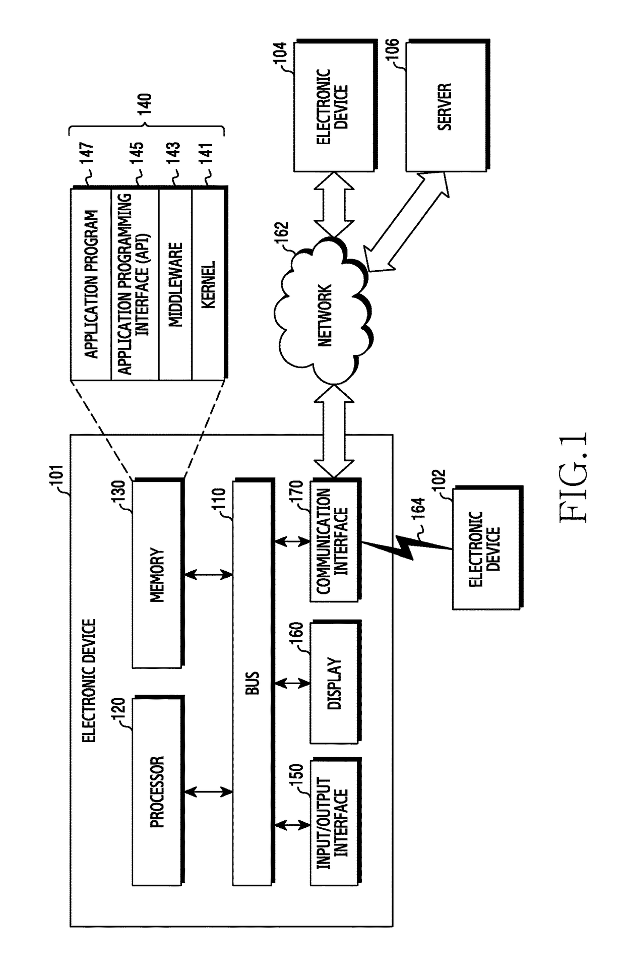
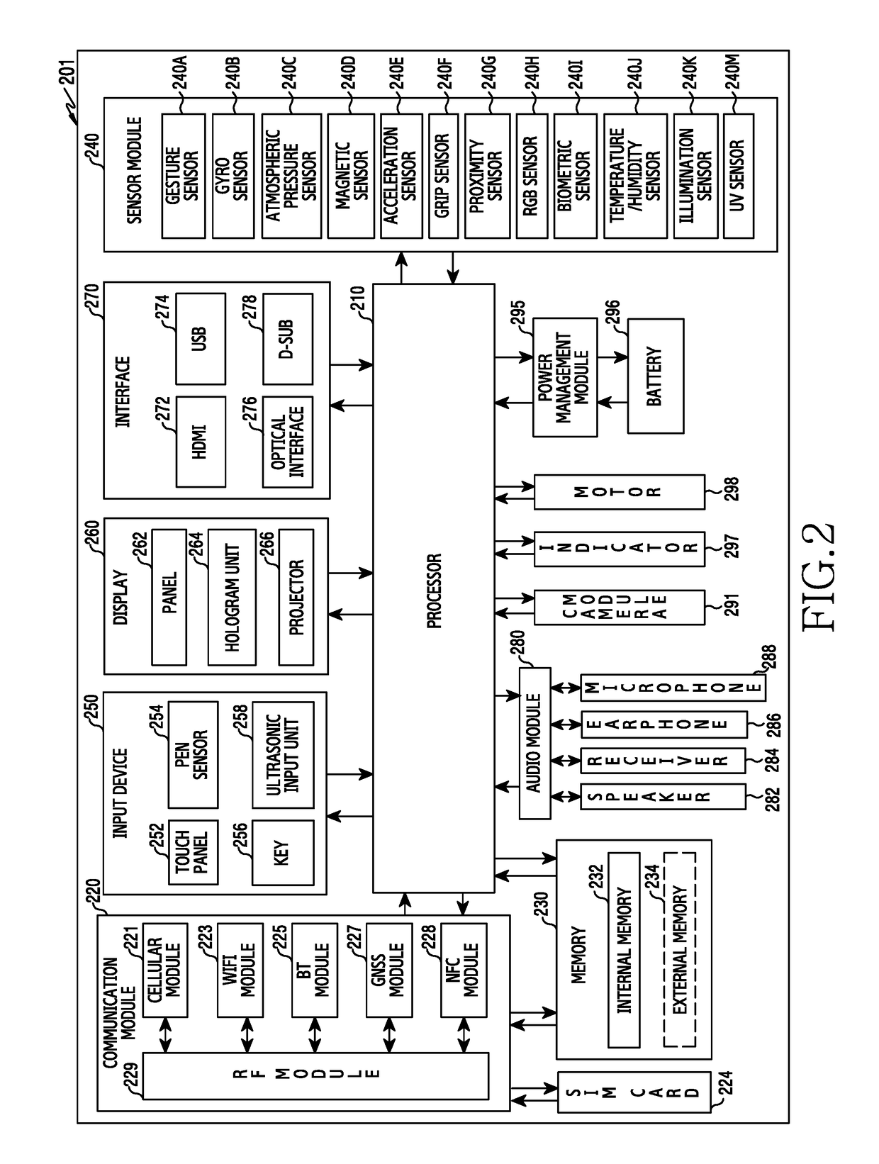
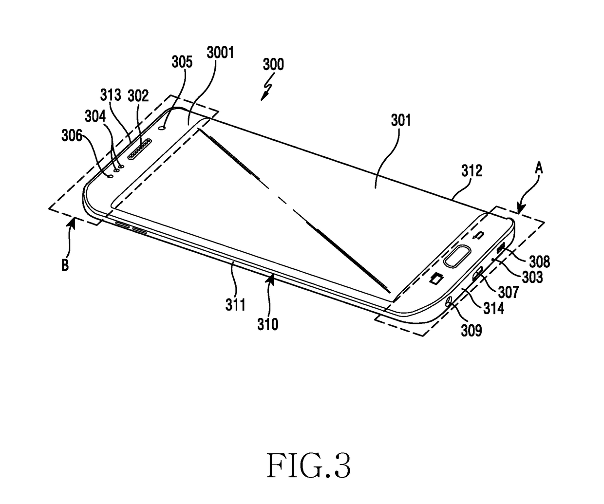
example electronic
[0040 devices may include smart phones, tablet personal computers (PCs), mobile phones, video telephones, electronic book readers, desktop PCs, laptop PCs, netbook computers, workstations, servers, personal digital assistants (PDAs), portable multimedia players (PMI's), Motion Picture Experts Group (MPEG-1 or MPEG-2) Audio Layer 3 (MP3) players, mobile medical devices, cameras, and / or wearable devices, or the like, but are not limited thereto. For example, the wearable devices may include accessory-type wearable devices (e.g., watches, rings, bracelets, anklets, necklaces, glasses, contact lenses, or head-mounted-devices (HMDs)), fabric or clothing integral wearable devices (e.g., electronic clothes), body-mounted wearable devices (e.g., skin pads or tattoos), and / or implantable wearable devices (e.g., implantable circuits), or the like but are not limited thereto.
[0041]The electronic devices may include smart home appliances, such as televisions (TVs), digital versatile disk (DVD) ...
PUM
 Abstract
Description
Claims
Application Information