Electronic devices with low refresh rate display pixels

a display and display technology, applied in the field of electronic devices with displays, can solve the problems of inadequately addressing all threshold voltage variations, unsatisfactory display artifacts, display to exhibit a low response time, etc., and achieve the effects of reducing flicker, preventing noticeable luminance dimming, and reducing threshold voltage hysteresis

Active Publication Date: 2019-05-28
APPLE INC
View PDF9 Cites 8 Cited by
  • Summary
  • Abstract
  • Description
  • Claims
  • Application Information

AI Technical Summary

Benefits of technology

[0008]The display pixel may be refreshed using a four-phase refresh scheme, which includes an initialization phase during which only the first scan signal and the second emission signal are asserted, an on-bias stress phase during which only the second scan signal is asserted, a threshold voltage sampling and data writing phase during which only the first and second scan signals are asserted, and an emission phase during which only the first and second emission signals are asserted. Performing the on-bias stress phase before the threshold voltage sampling and data writing phase can help mitigate threshold voltage hysteresis of the second transistor, which prevents first frame dimming (e.g., prevents noticeable luminance dimming when the pixel is transitioning from displaying a black level to a white level).
[0009]This type of display pixel may also be suitable for operati

Problems solved by technology

Threshold voltage variations in the thin-film transistors can cause undesired visible display artifacts.
This type of history-dependent behavior of the light output of the display pixels in a display causes the display

Method used


Image

  • Electronic devices with low refresh rate display pixels
  • Electronic devices with low refresh rate display pixels
  • Electronic devices with low refresh rate display pixels

Examples


Embodiment Construction

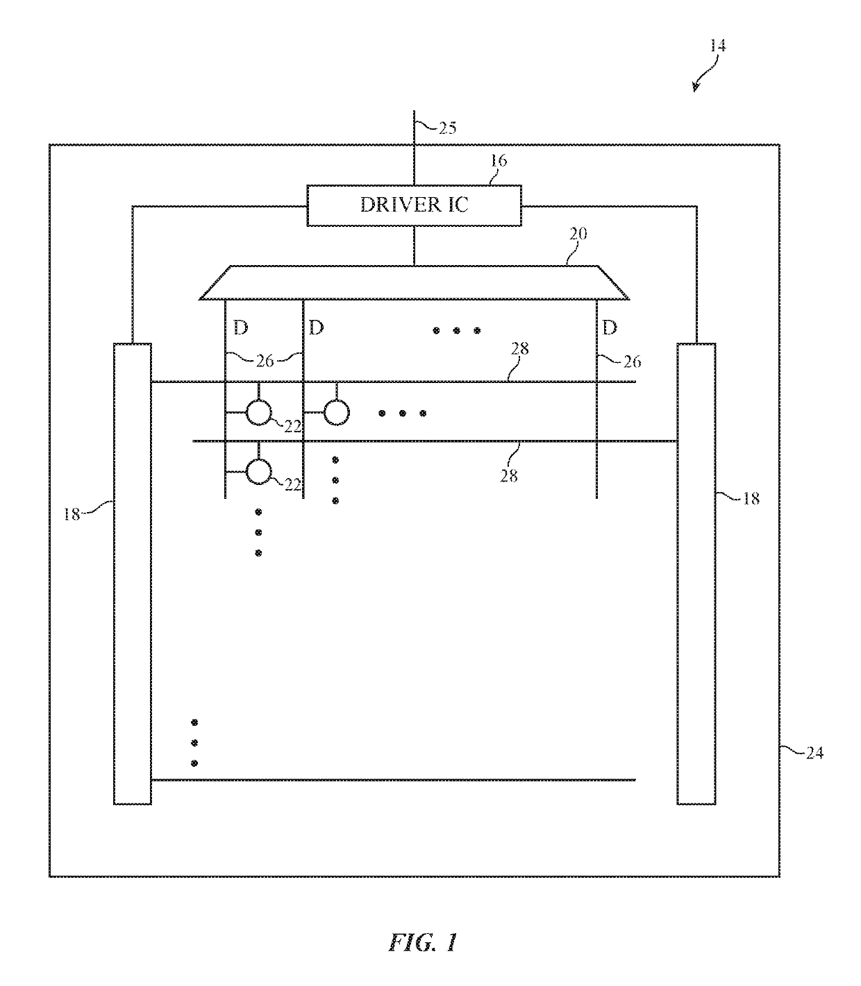
[0025]A display in an electronic device may be provided with driver circuitry for displaying images on an array of display pixels. An illustrative display is shown in FIG. 1. As shown in FIG. 1, display 14 may have one or more layers such as substrate 24. Layers such as substrate 24 may be formed from planar rectangular layers of material such as planar glass layers. Display 14 may have an array of display pixels 22 for displaying images for a user. The array of display pixels 22 may be formed from rows and columns of display pixel structures on substrate 24. These structures may include thin-film transistors such as polysilicon thin-film transistors, semiconducting oxide thin-film transistors, etc. There may be any suitable number of rows and columns in the array of display pixels 22 (e.g., ten or more, one hundred or more, or one thousand or more).

[0026]Display driver circuitry such as display driver integrated circuit 16 may be coupled to conductive paths such as metal traces on ...


PUM


Abstract

A display may have an array of organic light-emitting diode display pixels operating at a low refresh rate. Each display pixel may have six thin-film transistors and one capacitor. One of the six transistors may serve as the drive transistor and may be compensated using the remaining five transistors and the capacitor. One or more on-bias stress operations may be applied before threshold voltage sampling to mitigate first frame dimming. Multiple anode reset and on-bias stress operations may be inserted during vertical blanking periods to reduce flicker and maintain balance and may also be inserted between successive data refreshes to improve first frame performance. Two different emission signals controlling each pixel may be toggled together using a pulse width modulation scheme to help provide darker black levels.

Description

[0001]This application claims the benefit of provisional patent application No. 62 / 547,030, filed Aug. 17, 2017, which is hereby incorporated by reference herein in its entirety.FIELD[0002]This relates generally to electronic devices and, more particularly, to electronic devices with displays.BACKGROUND[0003]Electronic devices often include displays. For example, cellular telephones and portable computers include displays for presenting information to users.[0004]Displays such as organic light-emitting diode displays have an array of display pixels based on light-emitting diodes. In this type of display, each display pixel includes a light-emitting diode and thin-film transistors for controlling application of a signal to the light-emitting diode to produce light.[0005]Threshold voltage variations in the thin-film transistors can cause undesired visible display artifacts. For example, threshold voltage hysteresis can cause white pixels to be displayed differently depending on contex...

Claims


Application Information

Patent Timeline
IPC IPC(8): G09G3/32G09G3/3225
CPCG09G3/3225G09G2300/0819G09G2310/061G09G2320/064G09G2320/0242G09G2320/0247G09G2320/0252G09G2320/0214G09G3/3208G09G3/3233G09G2310/0262G09G2310/0297G09G2300/0861G09G2300/0417G09G2300/043G09G2320/045G09G2320/043G09G2340/0435G09G2310/06
Inventor LIN, CHIN-WEIYANG, SHYUANQIAN, CHUANGJAMSHIDI ROUDBARI, ABBASCHANG, TING-KUO
Owner APPLE INC
Why Eureka
Try Eureka