Display panel

a technology of transistor array and display panel, which is applied in the field of display panel, can solve the problems of electrical performance decline and considerable effect on display quality, and achieve the effect of pixel size reduction

Active Publication Date: 2019-05-28
INNOLUX CORP
View PDF10 Cites 2 Cited by
  • Summary
  • Abstract
  • Description
  • Claims
  • Application Information

AI Technical Summary

Benefits of technology

[0005]The disclosure is related to a display panel, and a transistor structure design of a transistor array substrate of the embodiment maintains the electrical properties of the display panel with the decrease of the pixel size.

Problems solved by technology

The faulty design of the related components and layers of the display panel will lead to the decreases of the electrical performance, and have considerable effects on the displaying quality.

Method used


Image

  • Display panel
  • Display panel
  • Display panel

Examples


Embodiment Construction

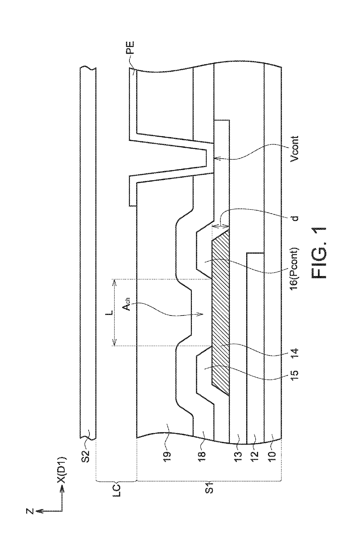
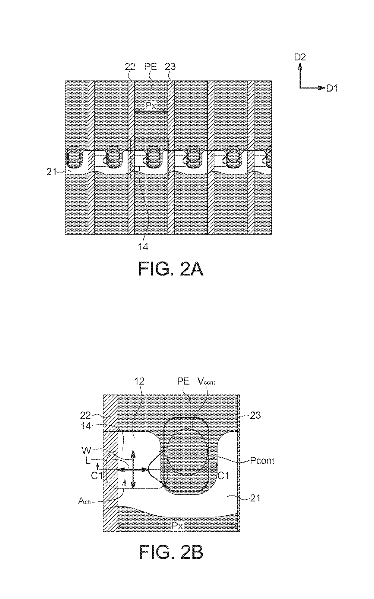
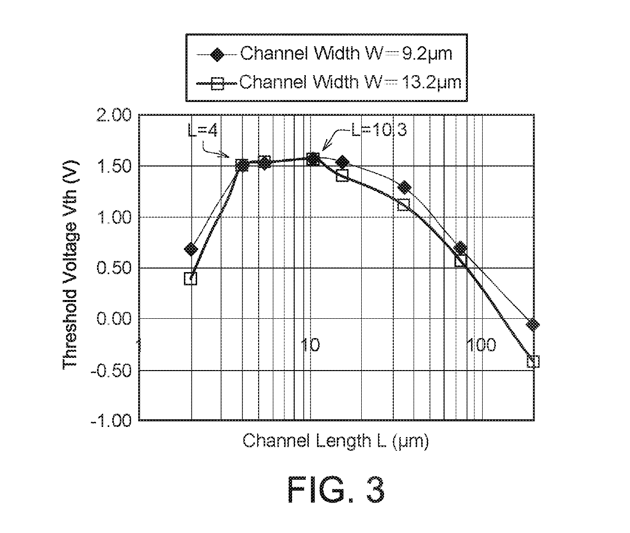
[0025]In the embodiment of the disclosure, a display panel having a transistor array substrate with a particular transistor structure design is provided. According to the embodied transistor structure design, the sizes of the feature parameters (such as the channel width and the channel length of the active layer) of the transistor can be reduced correspondingly with the decrease of the pixel size (ex: applied to a product with high resolution), and the electrical properties of the display panel are still well-maintained to satisfy the requirements of the commercial products in applications; for example, the charging capability and the load capacitance of the transistor have to meet the operating specifications of the product in application.

[0026]The embodiments are described in details with reference to the accompanying drawings. The embodiment of the disclosure can be applied to a liquid crystal display (LCD) panel having a back-channel-etch type thin film transistor (BCE-type TFT...


PUM

PropertyMeasurementUnit
lengthaaaaaaaaaa
widthaaaaaaaaaa
lengthaaaaaaaaaa

Abstract

A display panel includes a first substrate, and the first substrate includes a base plate; a first conductive line disposed on the base plate and extending along the first direction; a second conductive line and a third conductive line disposed on the base plate and extending along the second direction; a contact pad positioned between the second and third conductive lines; a semi-conductive layer connecting the contact pad and the second conductive line, and the semi-conductive layer having a thickness d; and a pixel electrode connecting the contact pad. The semi-conductive layer has a channel width W (μm) and a channel length L (μm) between the contact pad and the second conductive line, and a pixel distance Px (μm) between the second and third conductive lines along the first direction, wherein the channel width W is conformed to the following equation:(3.035-1.5)≤W-0.008×(Px×Ld)≤(3.035+1.5).

Description

[0001]This application claims the benefit of Taiwan application Serial No. 105106313, filed Mar. 2, 2016, the subject matter of which is incorporated herein by reference.BACKGROUNDField of the Invention[0002]The disclosure relates in general to a display panel, and more particularly to a transistor structure of a transistor array substrate of a display panel.Description of the Related Art[0003]Today, electronic products with display panels, such as smart phones, tablet personal computers (i.e. tablet PC, flat PC, ex: iPad), laptops, monitors, and televisions, are necessary tools for work and leisure in the daily life. Liquid crystal display (LCD) panel is the most popular display panel in use. For a LCD panel applicable to a flat display, an electronic visual display and an image display, the liquid crystal molecules aligned between two transparent electrodes rotate continuously depending on the polarity and magnitude of the electric field when the electric field is applied, and dif...

Claims


Application Information

Patent Timeline
Patent Type & Authority Patents(United States)
IPC IPC(8): H01L29/10H01L29/12H01L27/12H01L29/786G02F1/1362G02F1/1368H01L27/32
CPCH01L29/78696H01L27/124H01L27/1225H01L29/786H01L29/7869H01L29/78618H01L27/3276G02F1/1368G02F1/136227G02F1/136286H01L27/3248H01L27/3262H01L27/1222H10K59/123H10K59/131H10K59/1213
Inventor WANG, CHAO-HSIANGCHEN, YI-CHINGLEE, KUAN-FENGLIN, HSIN-HUNGYEH, SHOU-PUWU, YUAN-LIN
Owner INNOLUX CORP
Why Eureka
Try Eureka