Method for binding micro device to substrate

a technology of micro devices and substrates, applied in the direction of solid-state devices, electric devices, basic electric elements, etc., can solve the problem of one of the most challenging tasks

Active Publication Date: 2019-06-04
MIKRO MESA TECH
View PDF8 Cites 11 Cited by
  • Summary
  • Abstract
  • Description
  • Claims
  • Application Information

AI Technical Summary

Benefits of technology

[0004]According to some embodiments of the present disclosure, a method for binding a micro device to a substrate is provided. The method includes: locally showering a gas on a portion of the substrate, in which the gas has a water vapor pressure higher than an ambient water vapor pressure; and placing the micro device over the portion of

Problems solved by technology

Among all technical aspects of micro devices, transfer process is one of the most challenging tasks for micro devices

Method used


Image

  • Method for binding micro device to substrate
  • Method for binding micro device to substrate
  • Method for binding micro device to substrate

Examples


Embodiment Construction

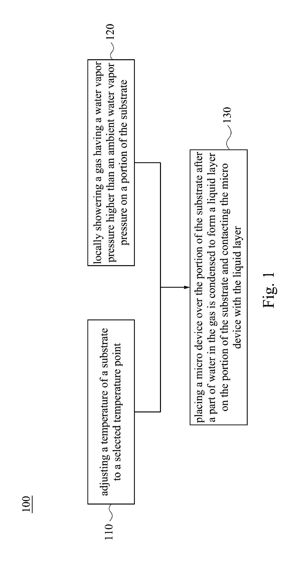
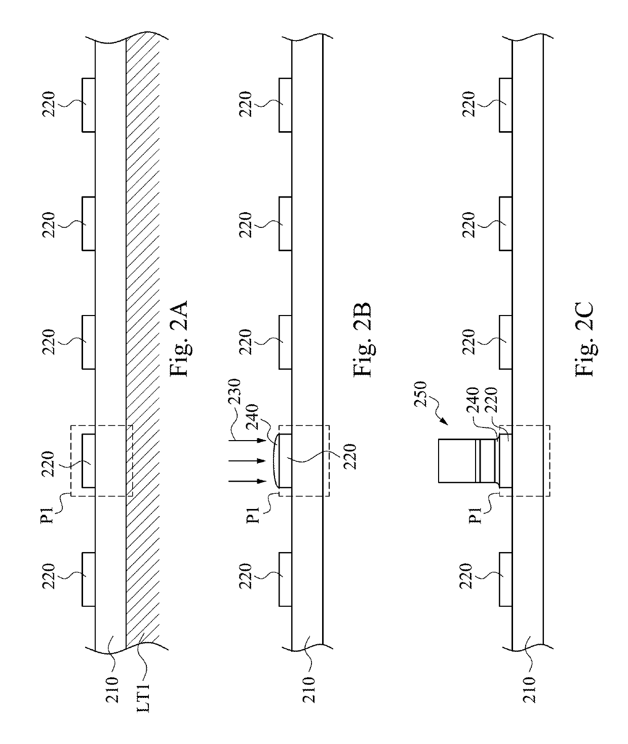
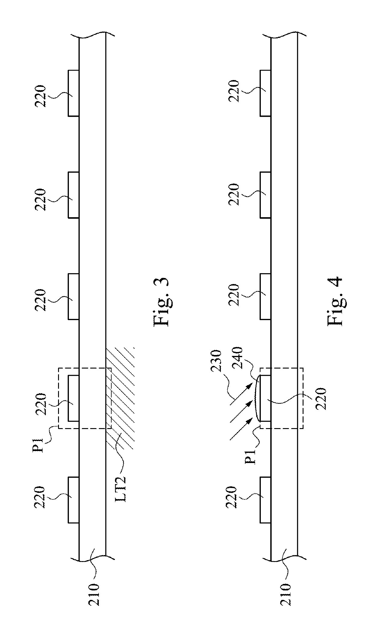
[0019]Reference will now be made in detail to the present embodiments of the disclosure, examples of which are illustrated in the accompanying drawings. Wherever possible, the same reference numbers are used in the drawings and the description to refer to the same or like parts.

[0020]In various embodiments, description is made with reference to figures. However, certain embodiments may be practiced without one or more of these specific details, or in combination with other known methods and configurations. In the following description, numerous specific details are set forth, such as specific configurations, dimensions and processes, etc., in order to provide a thorough understanding of the present disclosure. In other instances, well-known semiconductor processes and manufacturing techniques have not been described in particular detail in order to not unnecessarily obscure the present disclosure. Reference throughout this specification to “one embodiment,”“an embodiment”, “some emb...


PUM


Abstract

A method for binding a micro device to a substrate is provided. The method includes: locally showering a gas on a portion of the substrate, wherein the gas has a water vapor pressure higher than an ambient water vapor pressure; and placing the micro device over the portion of the substrate after a part of water in the gas is condensed to form a liquid layer on the portion of the substrate and contacting the micro device with the liquid layer, so that the micro device is gripped by a capillary force produced by the liquid layer and is substantially held in a position within a controllable region on the substrate.

Description

BACKGROUNDField of Invention[0001]The present disclosure relates to a method for binding a micro device to a substrate.Description of Related Art[0002]The statements in this section merely provide background information related to the present disclosure and do not necessarily constitute prior art.[0003]In recent years, micro devices have become popular in various applications. Among all technical aspects of micro devices, transfer process is one of the most challenging tasks for micro devices to be commercialized. One of the important issues of the transfer process is bonding the micro devices to a substrate.SUMMARY[0004]According to some embodiments of the present disclosure, a method for binding a micro device to a substrate is provided. The method includes: locally showering a gas on a portion of the substrate, in which the gas has a water vapor pressure higher than an ambient water vapor pressure; and placing the micro device over the portion of the substrate after a part of wat...

Claims


Application Information

Patent Timeline
IPC IPC(8): H01L23/00H01L33/62
CPCH01L24/83H01L33/62H01L24/32H01L2224/83102H01L2924/12041H01L2224/32227H01L2933/0066H01L2224/8302H01L2224/83002H01L2224/75501H01L2224/83098H01L2224/83093H01L2224/29111H01L2224/83097H01L2924/014H01L2924/00014
Inventor CHEN, LI-YI
Owner MIKRO MESA TECH
Why Eureka
Try Eureka