Semiconductor device

a technology of semiconductors and devices, applied in the direction of instruments, optical waveguide light guides, optical light guides, etc., can solve the problems of increasing optical loss, /b> of the core layer cr is accompanied by manufacturing difficulties, and the optical loss is high. achieve the effect of low optical loss

Active Publication Date: 2019-10-29
RENESAS ELECTRONICS CORP
View PDF3 Cites 0 Cited by
  • Summary
  • Abstract
  • Description
  • Claims
  • Application Information

AI Technical Summary

Benefits of technology

[0009]In this point, when the core layer is comprised of a linear portion and a curved portion, the refractive index difference is preferably different depending on the shape of the core layer from the standpoint of reducing scattering loss, more specifically, the optimum refractive index difference between the core layer and the clad layer at the linear portion is preferably different from that between the core layer and the clad layer at the curved portion. To achieve this, formation of an optical waveguide different in refractive index between the clad layer that covers the core layer configuring the linear portion and the refractive index of the clad layer that covers the core layer configuring the curved portion can be considered as one measure. As a result of investigation, however, the present inventors have found newly that in the case where the refractive index of the clad layers that cover the core layer changes drastically in a direction of light propagating in the optical waveguide, optical loss is incurred due to scattering of light at the interface between the clad layers having respectively different refractive indices. This means that there is a room for improvement in achieving a low-loss optical waveguide having a core layer comprised of a linear portion and a curved portion.
[0012]Above-described embodiment can provide a semiconductor device including an optical waveguide capable of propagating light therein with low optical loss.

Problems solved by technology

The greater this evanescent light, the higher the optical loss.
Occurrence of scattering of light means an increase in optical loss by this new mechanism.
Realization of the first characteristic at both the upper surface and the side surface of the boundary portion P2 of the core layer CR is however accompanied with manufacturing difficulty.
On the other hand, it is difficult to, after application of a resist film onto the side surface, expose the resist film applied to the side surface to light and is therefore difficult to pattern the clad layer CLD1 into an intended shape by photolithography at the side surface of the boundary portion P2 of the core layer CR.

Method used


Image

  • Semiconductor device
  • Semiconductor device
  • Semiconductor device

Examples


first embodiment

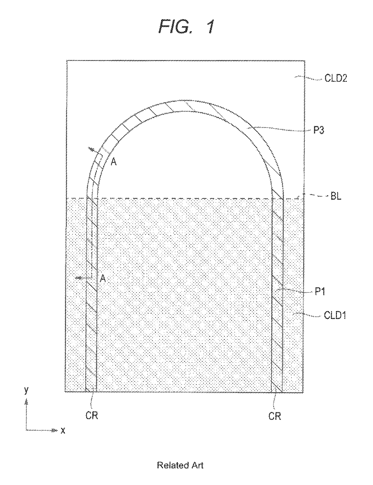
[0052]First, after description of the related art, room for improvement which the related art has will be described. A technical concept of First Embodiment for reducing the room for improvement of the related art will next be described.

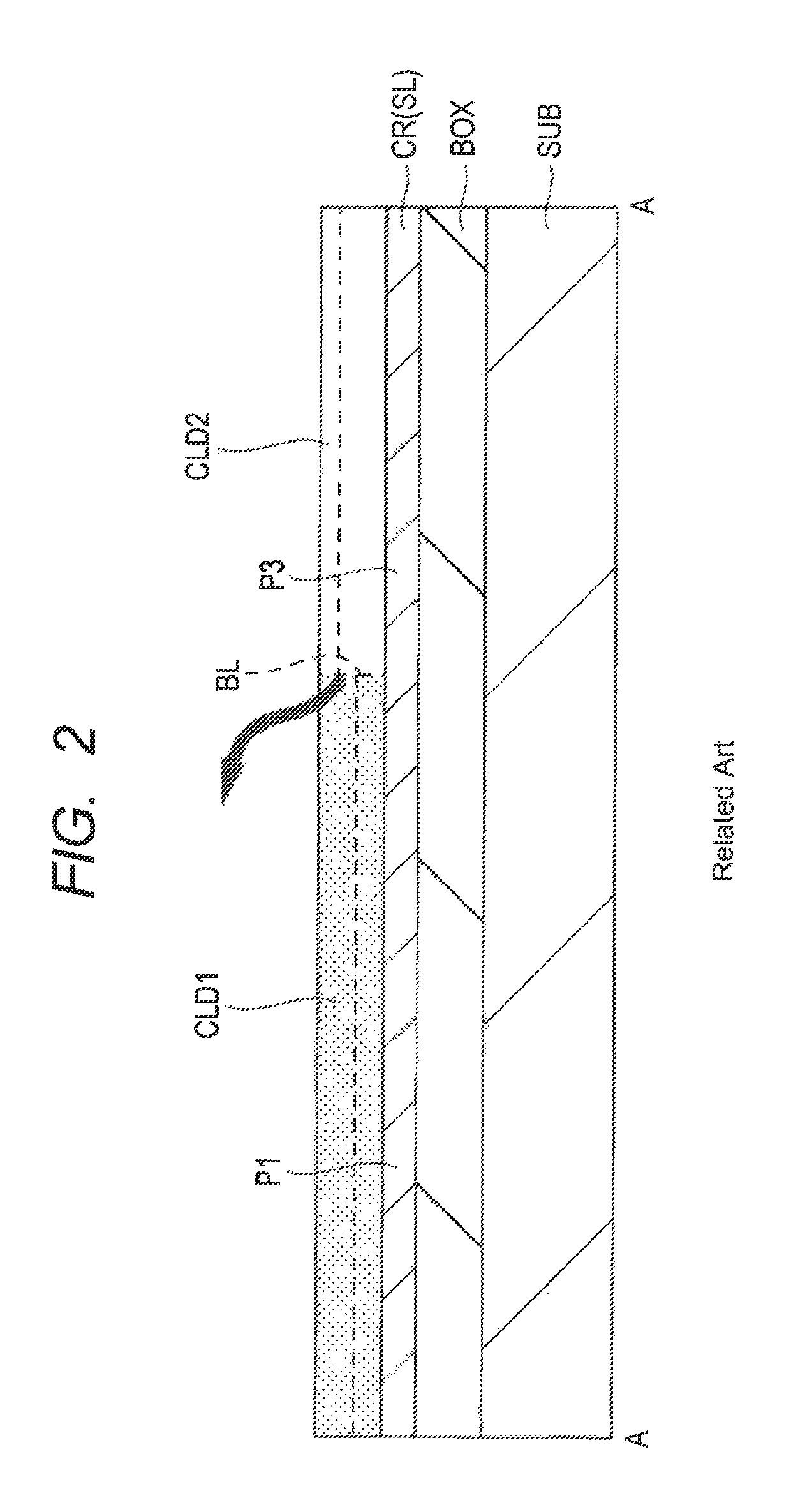
[0053]FIG. 1 shows a schematic configuration of an optical waveguide of the related art. The optical waveguide of the related art shown in FIG. 1 has a core layer CR formed on a substrate (refer to FIG. 2 described later). As shown in FIG. 1, this core layer CR is comprised of a linear portion P1 extending in a y direction (first direction) and a curved portion P3 having a finite radius of curvature. In FIG. 1, a boundary line BL for discriminating the linear portion P1 from the curved portion P3 is shown. This means that in FIG. 1, the linear portion P1 of the core layer CR is present below the boundary line BL in this drawing and the curved portion P3 of the core layer CR is present above the boundary line BL on this drawing. As shown in FIG. 1, a ...

modification example 1

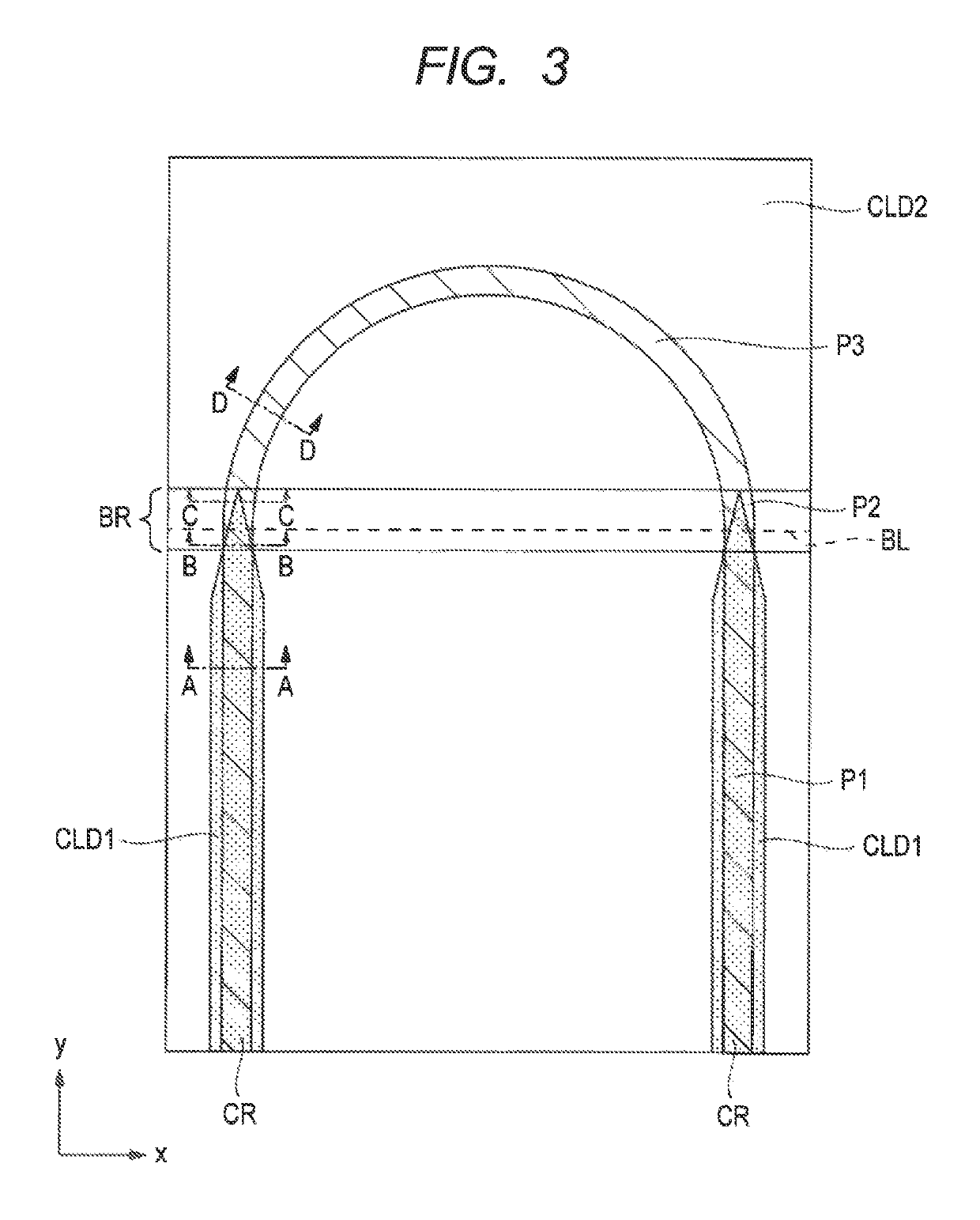
[0093]Modification Example 1 of First Embodiment will next be described. For example, in the optical waveguide of First Embodiment shown in FIG. 3, the boundary portion P2 of the core layer CR extends across the boundary line BL between the linear portion P1 of the core layer CR and the curved portion P3 of the core layer CR. The technical concept of First Embodiment is not limited to it but allows, for example, the boundary portion P2 of the core layer CR to be comprised of a portion extending below the boundary line BL of this drawing in the y direction (first direction), as shown in FIG. 8. In other words, the boundary portion P2 of the core layer CR may be comprised only of a portion of the linear portion P1. Alternatively, as shown in FIG. 9, the boundary portion P2 of the core layer CR may be comprised of a portion having a finite radius of curvature above the boundary line BL in this drawing. In short, the boundary portion P2 of the core layer CR may be comprised only of a po...

modification example 2

[0094]Modification Example 2 of First Embodiment will next be described. In First Embodiment shown in FIG. 3, the region which is below the boundary line BL in this drawing and is other than the region that covers the linear portion P1 of the core layer CR has therein not the clad layer CLD1 but the clad layer CLD2. This means that in First Embodiment, in plan view, the clad layer CLD1 covers only the linear portion P1 of the core layer CR and the vicinity thereof (for example, the oozing region of evanescent light). In other words, in First Embodiment, the core layer CR has two separated linear portions P1 formed on the support substrate SUB and two clad layers CLD1 separated from each other cover these two linear portions P1, respectively.

[0095]On the other hand, FIG. 10 shows a schematic configuration of an optical waveguide of Modification Example 2. In the optical waveguide of Modification Example 2 shown in FIG. 10, different from the optical waveguide of First Embodiment show...


PUM


Abstract

To provide a semiconductor device including a low-loss optical waveguide. The optical waveguide included in the semiconductor device has a core layer covered with first and second clad layers having respectively different refractive indices. A portion of the core layer is covered at a first ratio, that is, a ratio of the first clad layer to the second clad layer and at the same time, a second ratio, that is, a ratio of the second clad layer to the first clad layer. At this time, the first ratio and the second ratio are each a finite value more than 0.

Description

CROSS-REFERENCE TO RELATED APPLICATIONS[0001]The disclosure of Japanese Patent Application No. 2017-170268 filed on Sep. 5, 2017 including the specification, drawings, and abstract is incorporated herein by reference in its entirety.BACKGROUND[0002]The present invention relates to a semiconductor device, for example, a technique effective when applied to a semiconductor device including an optical waveguide formed using silicon photonics technology.[0003]Japanese Unexamined Patent Application Publication No. 2000-66048 (Patent Document 1) describes a technique relating to a semiconductor device having a quartz-based optical waveguide having an optimum refractive index difference for each shape.[0004]Japanese Unexamined Patent Application Publication No. 2000-131547 (Patent Document 2) describes a technique, in an optical waveguide having a curved waveguide and a linear waveguide, of controlling the refractive index of a core for making a refractive index difference between a core an...

Claims


Application Information

Patent Timeline
Patent Type & Authority Patents(United States)
IPC IPC(8): G02B6/122G02B6/125G02B6/12
CPCG02B6/1228G02B6/125G02B2006/12119G02B2006/12061
Inventor IIDA, TETSUYANAKASHIBA, YASUTAKA
Owner RENESAS ELECTRONICS CORP
Why Eureka
Try Eureka