Wiring structure and semiconductor package having the same
- Summary
- Abstract
- Description
- Claims
- Application Information
AI Technical Summary
Benefits of technology
Problems solved by technology
Method used
Image

Examples
Embodiment Construction
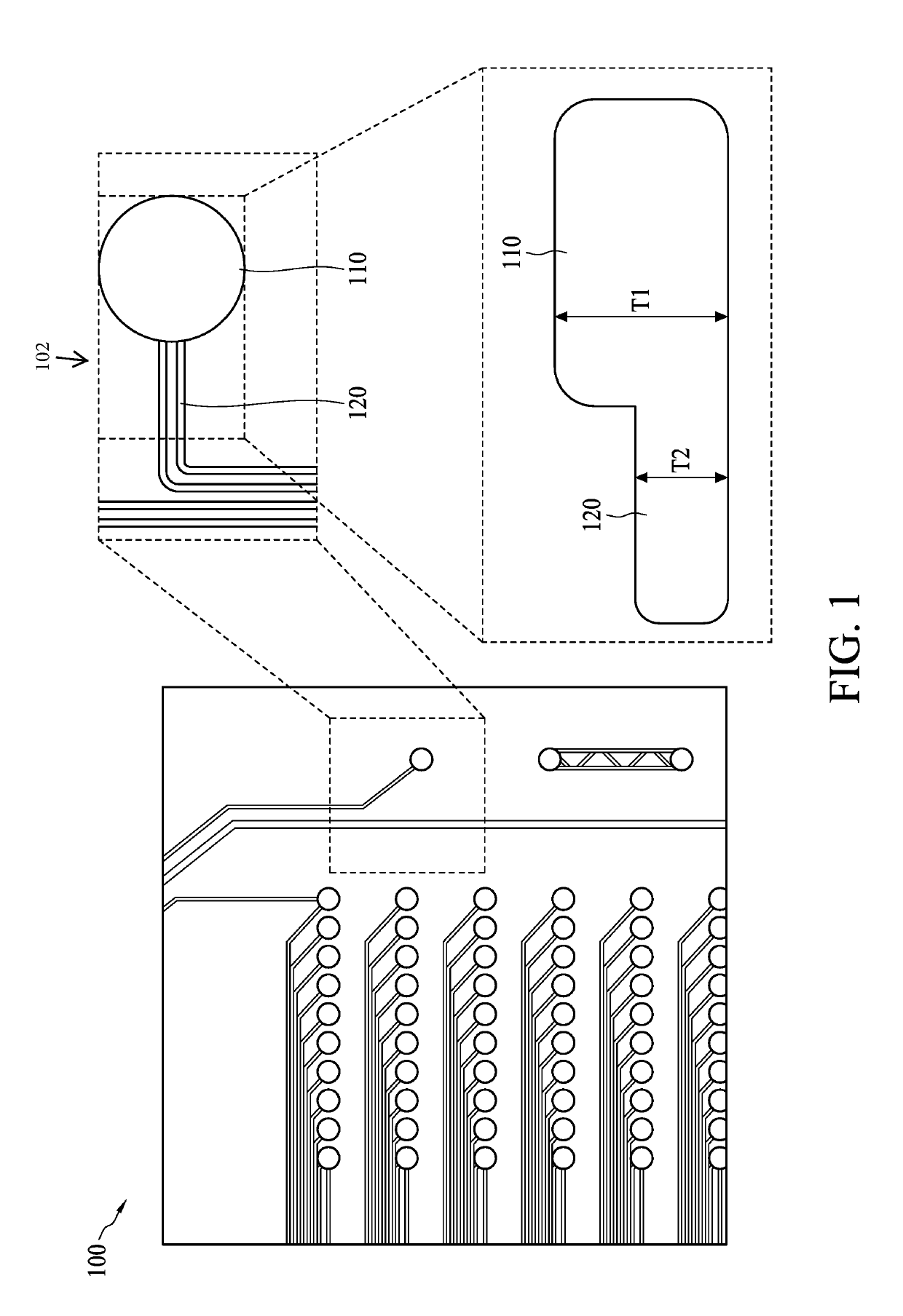
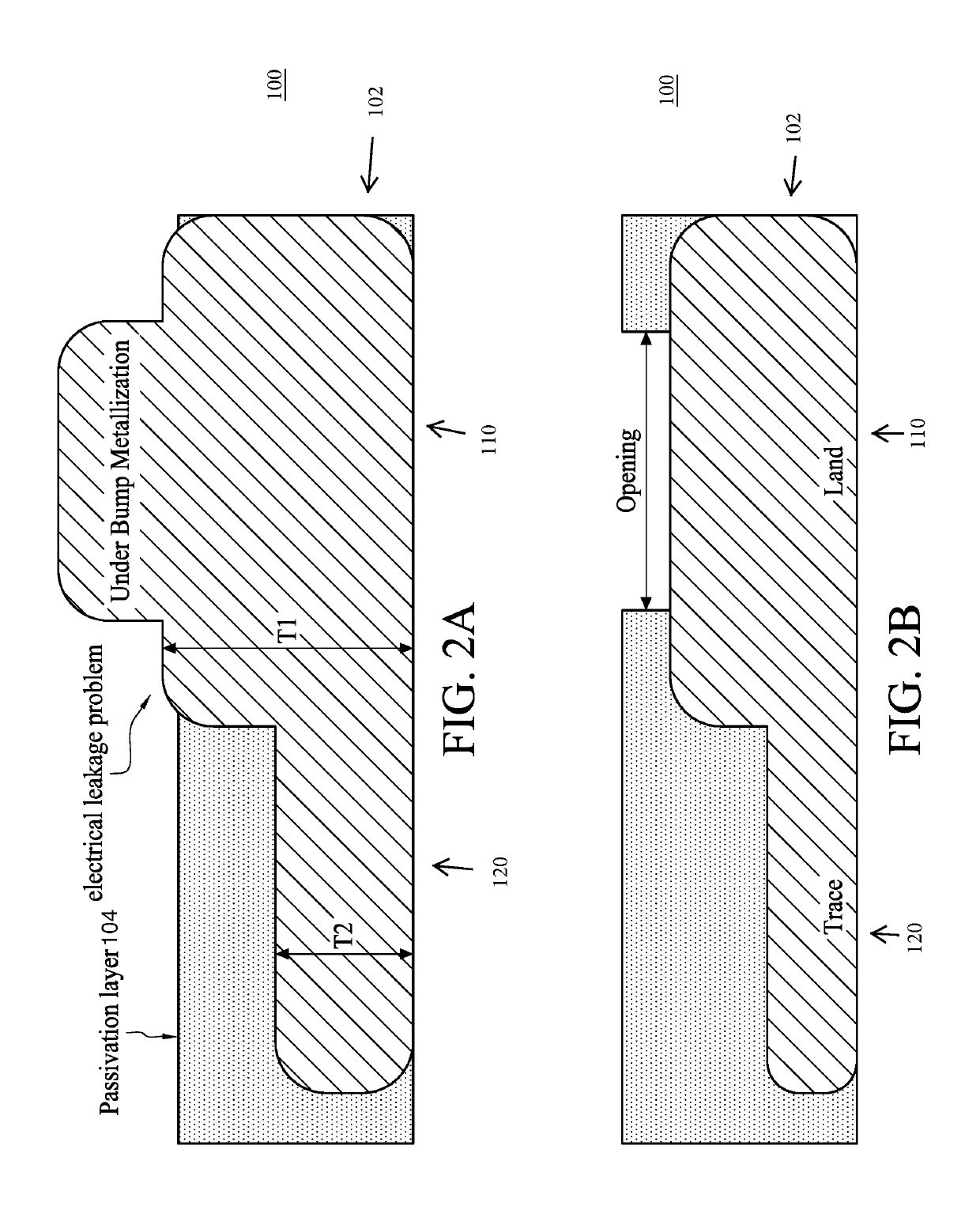
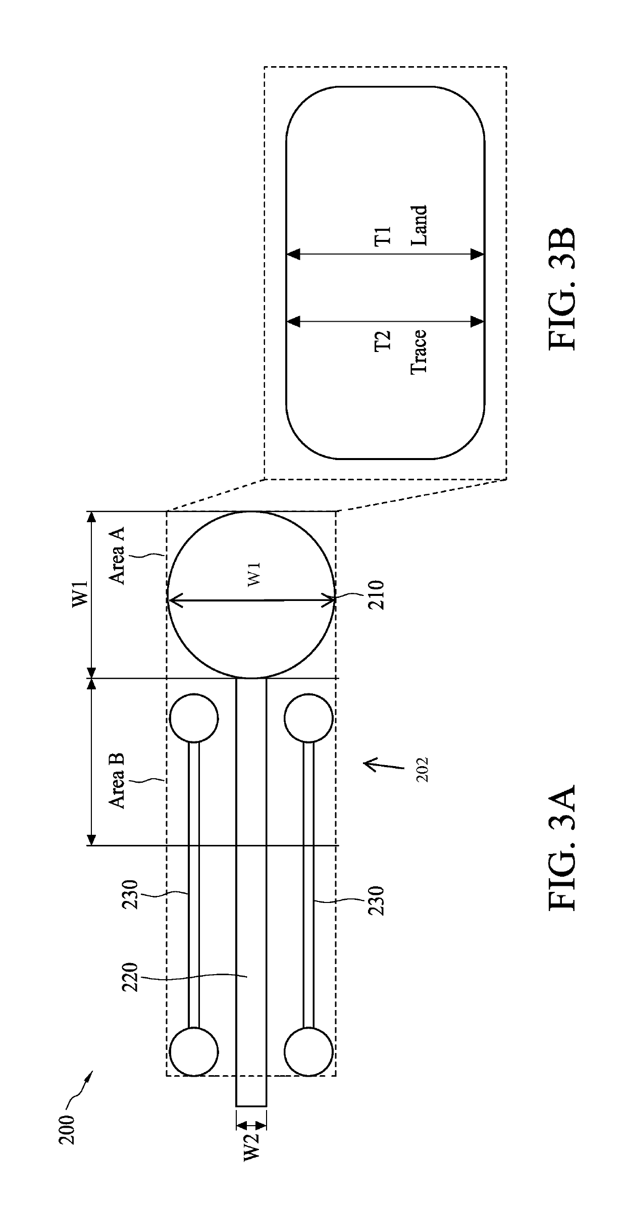
[0020]FIG. 1 shows a top view of a wiring structure 100 in accordance with some comparative designs of a wiring structure. As shown in FIG. 1, the wiring structure 100 includes a first wiring pattern 102. Shown at the upper right side of FIG. 1 is a magnified view of a portion of the wiring structure 100. The first wiring pattern 102 includes one or more conductive lands 110 and one or more conductive traces 120. Shown at the lower right side of FIG. 1 is a cross-sectional view of the magnified portion of the wiring structure 100. A thickness of one of the conductive lands 110 is T1 and a thickness of the conductive traces 120 is T2. The plating uniformity U can be calculated, for example, by the formula: U=(T1 (the thickness of the conductive land)−T2 (the thickness of the conductive traces)) / (2*(average of T1 and T2))*100%. For example, if after plating, T1 is about 4 μm and T2 is about 2 μm, the plating uniformity U is about: U=(4 μm−2 μm) / (2*((4 μm+2 μm) / 2))*100%=33.3%. This can...
PUM
 Abstract
Description
Claims
Application Information
PatSnap Eureka turns technology decisions into work you can execute. Powered by our Innovation Knowledge Graph, it runs expert workflows across engineering, life sciences, materials and intellectual property. Get your review-ready output in minutes.


