Antenna system and method for manufacturing an antenna system

a technology of antenna system and antenna system, which is applied in the direction of resonant antenna, individually energised antenna array, protective material radiating elements, etc., can solve the problems of complex technical aspects of high frequency suitable substrates, difficult integration into standardized manufacturing processes, and multi-layer substrate assemblies which include multiple substrate layers

Active Publication Date: 2019-11-05
ROBERT BOSCH GMBH
View PDF20 Cites 6 Cited by
  • Summary
  • Abstract
  • Description
  • Claims
  • Application Information

AI Technical Summary

Benefits of technology

[0015]According to the present invention, antenna systems having an increased bandwidth may be provided, in particular when the antenna system has a fixed surface area, whereby processes that are complicated and technically difficult to manage may advantageously be avoided.
[0018]According to one preferred refinement, the carrier device is made of the electrical insulation material. The carrier device in particular includes neither a material that is an electrical conductor nor a material that is an electrical semiconductor. The carrier device may thus have a particularly simple design, thereby reducing the manufacturing complexity and the susceptibility to errors.
[0020]According to another preferred refinement, the carrier device has a one-piece design. Manufacturing the carrier device is thus particularly easy to accomplish, and tolerances of the carrier device may be checked beforehand.
[0021]According to another preferred refinement, the carrier device is situated in part directly on the substrate, and in part spaced apart from the substrate. In particular, the carrier device together with the substrate may form a cavity having two wall surfaces facing one another, on whose first wall surface the first antenna structure is mounted, and on whose second wall surface the at least one second antenna structure is mounted. In addition, the carrier device may thus be directly adjusted with respect to the substrate, which is advantageous for meeting required tolerances.

Problems solved by technology

Substrates that are suitable for high frequencies are relatively complicated technically, and are often difficult to integrate into standardized manufacturing processes.
Multilayer substrate assemblies, which include multiple substrate layers suitable for high frequencies with etched structures, are often technically complex and involve a high level of manufacturing effort.

Method used


Image

  • Antenna system and method for manufacturing an antenna system
  • Antenna system and method for manufacturing an antenna system
  • Antenna system and method for manufacturing an antenna system

Examples


Embodiment Construction

[0034]Unless stated otherwise, identical or functionally equivalent elements and devices are provided with the same reference numerals in all figures. The numbering of method steps is for clarity, and unless stated otherwise, in particular is not intended to imply a specific chronological sequence. In particular, multiple method steps may be carried out at the same time.

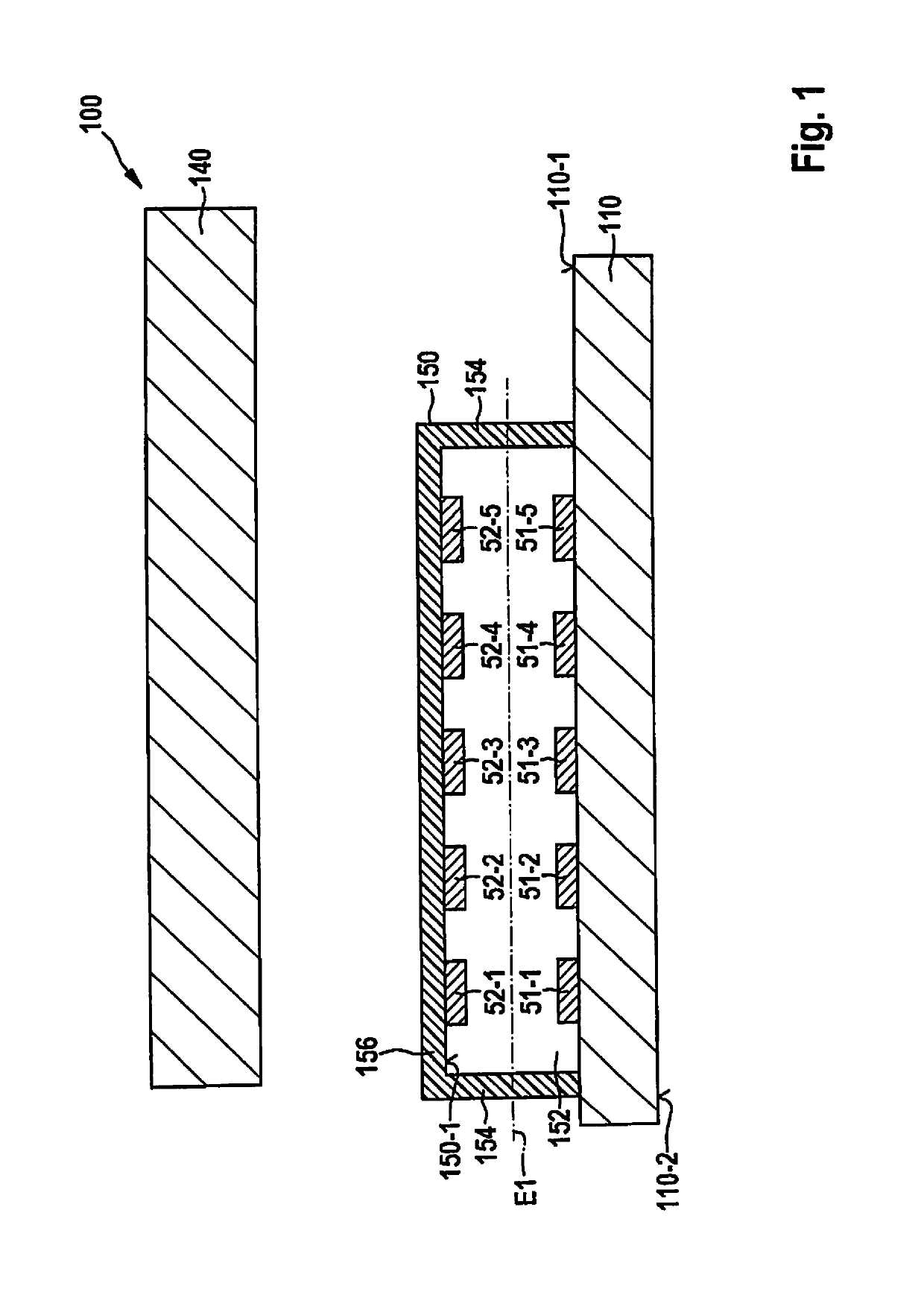
[0035]FIG. 1 shows a schematic cross-sectional view of an antenna system 100 according to one specific embodiment of the present invention.

[0036]As shown in FIG. 1, antenna system 100 includes a substrate 110 having a first outer side 110-1 on which a first antenna structure 51-1, 51-2, 51-3, 51-4, 51-5 is mounted. The first antenna structure includes individual first patch elements 51-1, 51-2, 51-3, 51-4, and 51-5, collectively denoted below as reference numeral 51-i, in microstrip technology, which in particular are flatly formed on first outer side 110-1. First antenna structure 51-i may, for example, be fed with ...


PUM


Abstract

An antenna system and a method for manufacturing same. The antenna system includes a substrate having a first outer side on which a first antenna structure is mounted; a radome spaced apart from the substrate on the first outer side of the substrate; a carrier device situated between the substrate and the radome which includes an insulating material; and at least one second antenna structure mounted on the carrier device which is spaced apart from the substrate and the radome.

Description

FIELD[0001]The present invention relates to an antenna system and a method for manufacturing an antenna system.BACKGROUND INFORMATION[0002]Radar sensors, which are often used for detecting the surroundings in vehicles with modern driver assistance systems, are operated in the frequency band of 76-77 GHz, for example. Enhanced radar sensors may have an extended frequency range of 76 GHz to 81 GHz, for example. Advantages of this increased available bandwidth are, for example, an increased spatial separation capability or the option for operating the radar sensor in different ranges of the frequency band in order to avoid disturbances due to interference by other radar sensors in the immediate vicinity.[0003]In conventional radar sensors, irradiation of electromagnetic waves as radar waves is generally achieved using so-called patch antennas in the microstrip line technology. In the simplest case, a rectangular metal-plated antenna element (also referred to as a patch element) is situ...

Claims


Application Information

Patent Timeline
Patent Type & Authority Patents(United States)
IPC IPC(8): H01Q1/38H01Q1/40H01Q9/04H01Q21/00H01Q23/00H01Q1/32H01Q21/06
CPCH01Q1/38H01Q21/0087H01Q9/0414H01Q1/405H01Q21/0075H01Q23/00H01Q21/065H01Q1/3233
Inventor KUGLER, ANDREASMEYER, JOHANNESSEIZ, JUERGENBAUR, KLAUSMAYER, MARCELKHAN, OSAMAFISCHER, ALEXANDER
Owner ROBERT BOSCH GMBH
Why Eureka
Try Eureka