Method of manufacturing an LED module

a manufacturing method and led module technology, applied in the direction of basic electric elements, electrical apparatus, semiconductor devices, etc., can solve the problems of unsuitable flexible led modules, titanium dioxide reduces the flexibility of silicone encapsulants, and unnecessary light loss in any region that is not in direct proximity, etc., to achieve fine control, improve the effect of encapsulant layer surface stability, and improve the effect of encapsulant flexibility

Active Publication Date: 2020-02-04
LUMILEDS
View PDF6 Cites 0 Cited by
  • Summary
  • Abstract
  • Description
  • Claims
  • Application Information

AI Technical Summary

Benefits of technology

[0012]An advantage of the LED module according to the invention is that it can appear as single light source even if it comprises many LEDs. Furthermore, since the scattering of the light is effected at an outer surface of an encapsulant layer, without the need for embedding any scattering particles inside the encapsulant material, the encapsulant be made entirely of a flexible silicone. This in turn means that the LED module itself can be flexible, allowing the LED module to assume essentially any shape.
[0014]An advantage of the device according to the invention is that the LED module can provide a favourably homogenous light output, appearing as a single light source. Because the LED module can be made to assume essentially any form, the device can include such an LED module that has an unusual shape, or a shape that would otherwise not be possible using a prior art approach to achieve a homogenous light source effect.
[0016]In the following, without restricting the invention in any way, it may be assumed that the translucent encapsulant comprises a silicone material. The modified surface structure of an encapsulant layer can be achieved using any suitable technique. For example, a fine milling tool could be used to form a desired pattern in the surface of an encapsulant layer. Preferably, the extent of each scattering region and / or the density of each scattering region is determined on the basis of a desired optical appearance of the LED module during operation. The inventive method makes it possible to create a “fading” scattering pattern, i.e. a high-density pattern over or above an LED, fading to a low-density pattern with increasing distance outward from the LED (when looking onto the light-emitting surface of the LED module). In a particularly preferred embodiment of the invention, the scattering patterns are created by an infrared laser light beam. For example, a laser with a wavelength in the region of 10 μm can be used to create different pattern regions as desired. In this way, the optical properties of the encapsulant layer surface are altered or modified, for example by deliberately altering the layer surface morphology, by locally changing the refractive index, etc. The use of a laser such as an infrared laser allows essentially any scattering pattern to be formed on the surface of silicone can be realised, in a pattern freely chosen to suit the requirements of an application using that LED module.
[0017]The scattering pattern can be achieved by making randomly placed alterations in the surface of the layer, closer together or further apart, depending on whether a densely patterned region or a sparsely patterned region is being created. However, in a preferred embodiment of the invention, a scattering pattern comprises a regular formation of recesses in the surface of a layer. This allows more control over the actual level of scattering that will be achieved in the finished product. Preferably, a recess has an essentially circular shape and is created by directing a pulse of laser light at a specific point on the layer surface. Regardless of how the scattering patterns are created, the depth of a scattering pattern is preferably relatively shallow. Preferably, a recess formed at an outer surface of a layer is no deeper than 50 μm-200 μm.
[0018]Using a laser allows fine control over the pattern that is created. For example, in a preferred embodiment of the invention the surface structure of a layer is modified to form a two-dimensional grid pattern. The grid pattern can comprise tiny dents or recesses formed at predefined distances to each other in order to achieve the desired pattern density. Another advantage of using a laser to form the scattering pattern is that the high degree of precision and control can be applied to form scattering regions to show a specific image, for example a company logo or brand name, in the on-state and / or off-state of the LED module.
[0019]The scattering patterns may be formed only on the outermost surface of the encapsulant. This can be sufficient to achieve a desired scattering effect and a favourably homogenous light output appearance. In a further preferred embodiment of the invention, scattering patterns may be formed on the outermost surface of the encapsulant and also at an intermediate level. This is easily achieved when the encapsulant comprises two or more layers, for example a lower layer with an unmodified or smooth surface, applied directly over the LEDs, and a further layer applied on top of the lower layer. This outer layer can be treated to form scattering patterns on its lower surface (which will contact the outer surface of the lower layer) as well as on its upper surface (which is the outermost surface of the encapsulant). Such a two-sided patterned layer can exhibit angle-dependent effects, for example to change the degree of homogeneity of the light source as the viewing angle changes, to make an image or logo appear or disappear as the viewing angle changes, etc.

Problems solved by technology

This “spottiness” is due to the brightness of each LED and the necessary pitch between the LEDs, and is generally perceived as undesirable.
Since the scattering agent concentration must be chosen to provide the desired degree of scattering in the region optically close to an LED, the disadvantage of the known approaches is the unnecessary loss of light in any region that is not in the direct vicinity of an LED—for example regions between LEDs of an array, regions along the outer edges of an LED module, etc.
Another disadvantage of the known approaches is that a scattering agent such as titanium dioxide reduces the flexibility of the silicone encapsulant.
In addition to the problems mentioned above, such an approach would therefore not be suited for a flexible LED module.
Another problem associated with the filled silicone scattering layers described above is that these must be defined or configured early on in the design stage due to the requirements of the encapsulating process, essentially ruling out any late-stage adjustment of a silicone diffuser.
The use of a diffuser foil is also not suited to flexible LED lighting solutions since a foil are not truly flexible in all directions.

Method used


Image

  • Method of manufacturing an LED module
  • Method of manufacturing an LED module
  • Method of manufacturing an LED module

Examples


Embodiment Construction

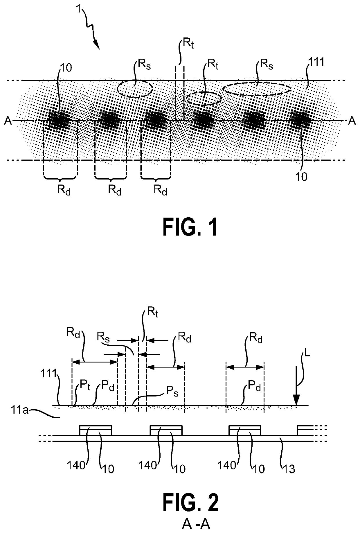
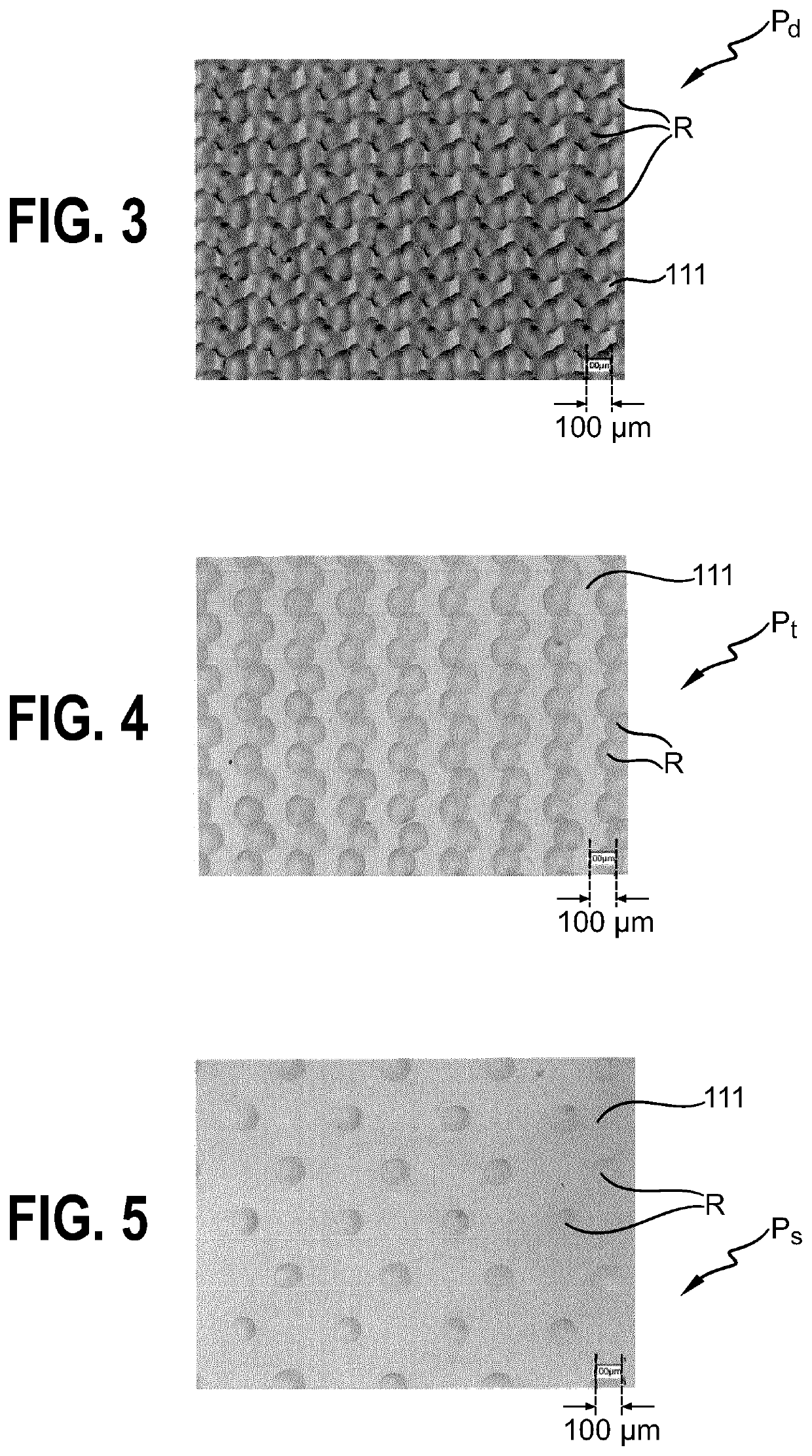
[0032]FIG. 1 shows a schematic representation of a view onto the light output surface 111 of an LED module 1 according to the invention. The LED module 1 comprises a series of LEDs 10 arranged in series on a carrier (not shown). The LEDs 10 are spaced apart by a certain pitch P. In this exemplary embodiment, the light output surface 111 is the uppermost surface 111 of a translucent encapsulant 11. The diagram indicates the outline of the LED dies 10 as seen through the transparent encapsulant. Scattering patterns Pd, Ps, Pt with different densities have been formed in specific regions Rd, Rs, Rt of the uppermost surface 111 to a depth of a few microns. The diagram schematically indicates the different pattern densities in the different regions Rd, Rs, Rt. Directly over an LED 10 and extending beyond the contours of the LED die, the scattering pattern Pd is dense. At the outer regions of the module's light output surface, the scattering pattern Ps is sparse. Between these regions, a ...


PUM

PropertyMeasurementUnit
wavelengthaaaaaaaaaa
thicknessaaaaaaaaaa
thicknessaaaaaaaaaa

Abstract

The invention describes a method of manufacturing an LED module, comprising the steps of providing a translucent encapsulant comprising a number of layers to enclose a number of LEDs of the LED module; modifying the surface structure of an outer surface of a layer to form at least one dense scattering region corresponding to the position of an LED of the LED module; to form at least one sparse scattering region that does not correspond to the position of an LED of the LED module; and to form a transition scattering region between a dense scattering region and a sparse scattering region. The invention further describes an LED module, and a device comprising a device housing and at least one such LED module.

Description

FIELD OF THE INVENTION[0001]The invention describes a method of manufacturing an LED module; an LED module; and a device incorporating such an LED module.BACKGROUND OF THE INVENTION[0002]Light-emitting diodes are used in a wide variety of applications. Specifically, high-power LEDs are finding widespread used in retrofit lamps; in automotive lighting modules such as daytime running lights, brake lights and indicator lights, etc. For linear lighting modules consisting of an array or series of individual LEDs positioned at a certain pitch, regions of concentrated high luminance light are observed when looking at the light source. This “spottiness” is due to the brightness of each LED and the necessary pitch between the LEDs, and is generally perceived as undesirable. Various approaches have been tried in order to obtain the appearance of a homogeneous light source when the light source in fact includes multiple LEDs. For example, a phosphor layer can reduce the inhomogeneity of the ap...

Claims


Application Information

Patent Timeline
Patent Type & Authority Patents(United States)
IPC IPC(8): H01L33/54H01L25/075
CPCH01L25/0753H01L33/54H01L2933/0091H01L33/22
Inventor SWEEGERS, NORBERTUS ANTONIUS MARIACROMPVOETS, FLORIS MARIA HERMANSZKLEIJNEN, CHRISTIANKUMS, GERARD
Owner LUMILEDS
Why Eureka
Try Eureka