
Electronic device and click pad thereof

a technology of electronic devices and click pads, which is applied in the field of click pads, can solve the problems of increasing production costs and assembly time, complicated production process of combining glass panels, circuit boards, restoration units and bottom brackets, etc., and achieves the effect of easy and fast production

Active Publication Date: 2020-02-18
CHICONY ELECTRONICS
View PDF6 Cites 0 Cited by
  • Summary
  • Abstract
  • Description
  • Claims
  • Application Information

AI Technical Summary

Benefits of technology

The present invention provides a click pad that has a streamlined structure, making it easy and fast to produce. An electronic device with the streamlined click pad is also provided. This simplifies the process of creating and manufacturing the click pad, improving efficiency and user experience.

Problems solved by technology

However, the production process of combining the glass panel, the circuit board, the restoration unit and the bottom bracket is very complicated.
Moreover, installing the additional grounding metal strip also increases the production cost and assembly time.

Method used


Image

  • Electronic device and click pad thereof
  • Electronic device and click pad thereof
  • Electronic device and click pad thereof

Examples


Embodiment Construction

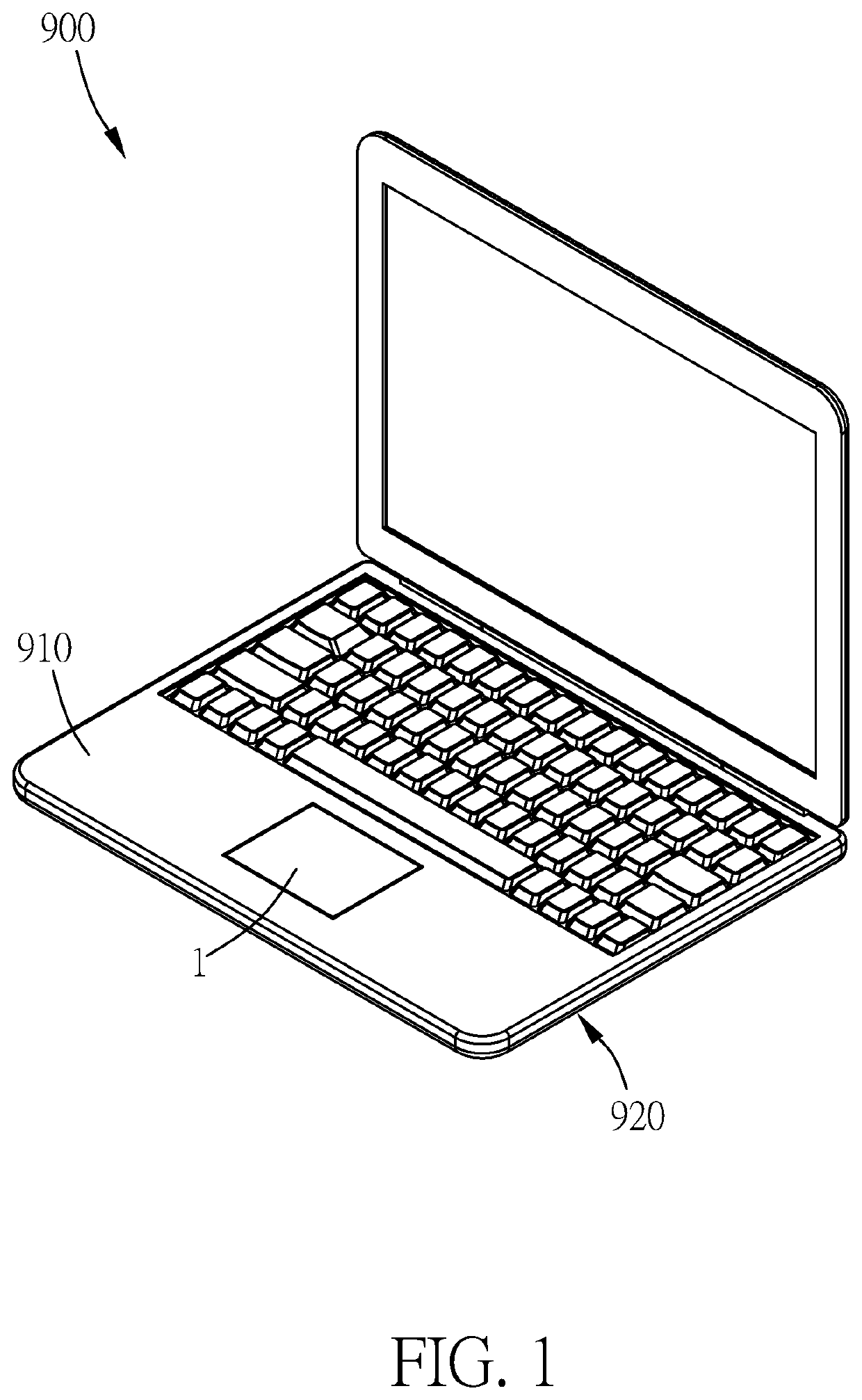
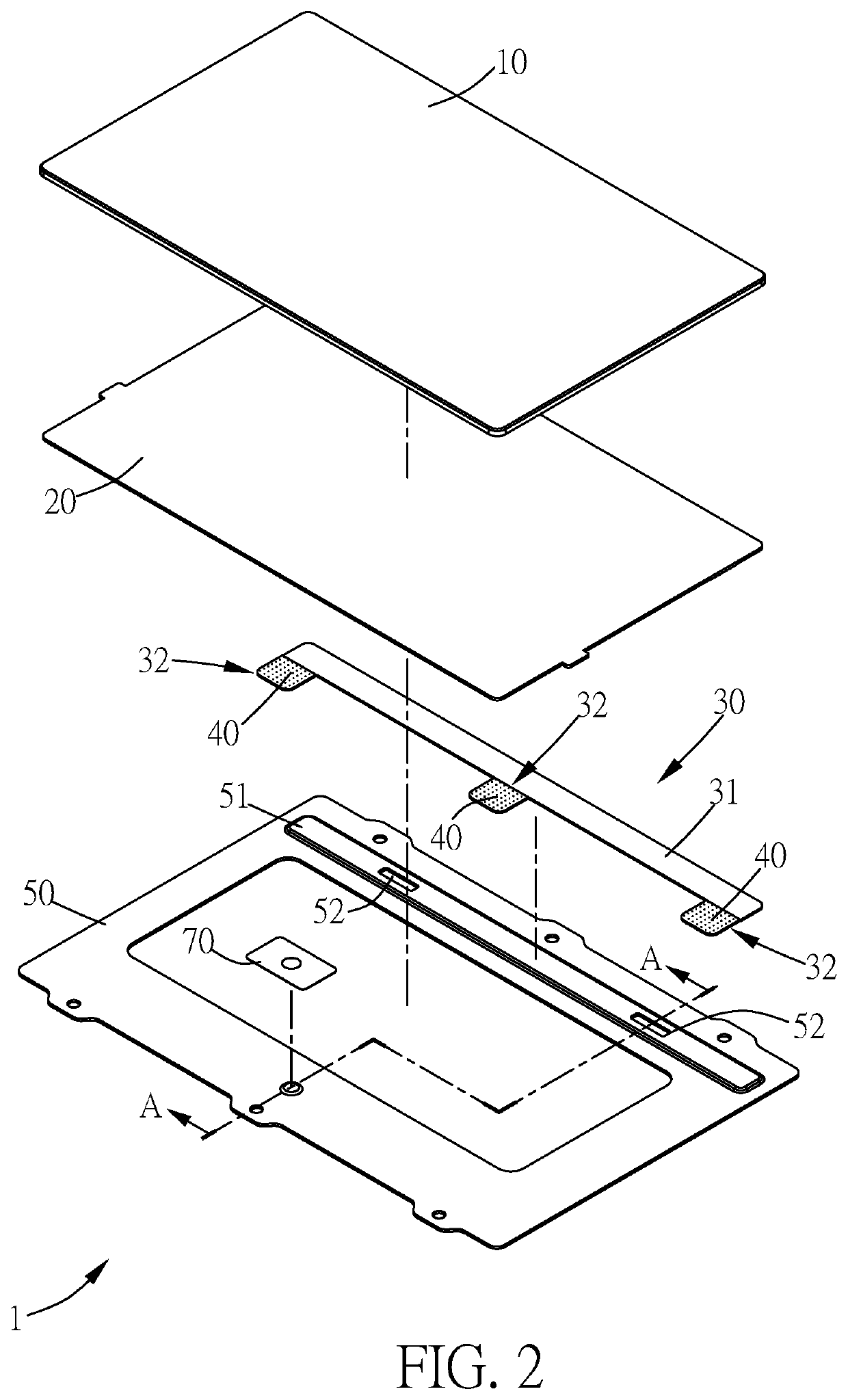
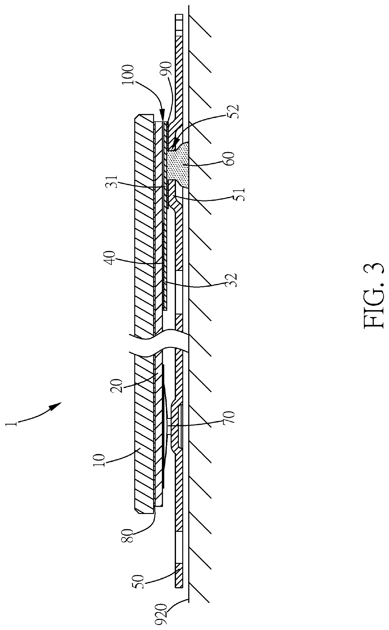
[0021]Please refer to FIG. 1 to FIG. 4, which illustrate the electronic device and the click pad thereof in the first embodiment of the present invention. FIG. 1 illustrates a schematic drawing of the electronic device in the first embodiment of the present invention. FIG. 2 illustrates an exploded drawing of the click pad in the first embodiment of the present invention. FIG. 3 illustrates a sectional view of the click pad in the first embodiment of the present invention along the section line AA shown in FIG. 2. FIG. 4 illustrates a bottom schematic drawing of the bottom bracket when the metal elastic board main body and the protruding part are combined in the first embodiment of the present invention.

[0022]As shown in FIG. 1 to FIG. 3, in the first embodiment of the present invention, the click pad 1 is a flat plate with touching and pressing function. The click pad 1 has a streamlined structure which is easy and fast to produce such that this structure of click pad 1 can save th...


PUM


Abstract

A click pad which is applied to an electronic device includes a top board, a circuit board, a metal elastic board, a conductive connection layer, a bottom bracket and a restoration unit. The circuit board is located under the top board and connected to the top board. The metal elastic board under the circuit board includes a metal elastic board main body and a connection part. A buffer gap is formed between the metal elastic board main body and the circuit board. The connection part connects to the metal elastic board main body. The conductive connection layer connects to the circuit board and the connection part. The bottom bracket under the metal elastic board includes a protruding part. The protruding part supports the metal elastic board main body. The restoration unit supports the circuit board.

Description

BACKGROUND OF THE INVENTION1. Field of the Invention[0001]The present invention relates to a click pad; more particularly, the present invention relates to a click pad which has a streamlined structure such that the click pad is easy and fast to produce.2. Description of the Related Art[0002]A common notebook computer usually has a click pad located below the keyboard board for allowing the user to use a finger to press the click pad or slide on the click pad to give a touch instruction to the notebook computer. When producing the click pad, a worker has to use an adhesive or fastener to combine the glass panel, the circuit board, the dome sheet and the bottom bracket to assemble the click pad, and also has to install an additional grounding metal strip between the circuit board and the bottom bracket so that excess electricity can be transferred to the outside of the click pad via the grounding metal strip.[0003]However, the production process of combining the glass panel, the circ...

Claims


Application Information

Patent Timeline
Patent Type & Authority Patents(United States)
IPC IPC(8): G06F1/16H05K1/02G06F3/0354
CPCG06F1/1656H05K1/0215G06F3/03547G06F1/169
Inventor UANG, KUANG-SHENCHANG, CHIA-WEISHI, GUO-YU
Owner CHICONY ELECTRONICS
Learn More